]Homework 3 // Due at Lecture Mon Feb 25
Primary contact for this
homework: Shengnan Wang [shengnan
at cs dot wisc dot edu].
You must do this homework individually. Please
submit your solutions in paper (no soft
copies) and staple multiple pages together. Please be sure to
include your section number, your name and email address on the first page.
Warning: Most homework will use questions from your
textbook, Patt and Patel's Introduction to
Computing Systems, which we abbreviate (ItCS) .
Problem 1
Draw a logic circuit corresponding to the following logic
expression. Your circuit must use only 2-input AND, 2-input OR, and NOT gates.
Z = ((A OR B) AND (NOT (C AND D))) OR (NOT (A) AND (E OR F))
Problem 2
Consider a
logic circuit which has four inputs A, B, C and D and an output Z. The output Z is 1 if
and only if the total number of 1s among A, B, C and D is strictly greater than 2 (not equal).
a. Draw a truth table for a logic circuit that performs this
function.
b. Write the logic expression corresponding to the
circuit.
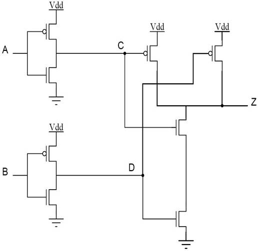
Problem 3
For the transistor-level
circuit in the figure below:
a. Fill in the truth table.
|
A B |
C
D Z |
|
|
|
b. What is
Z in terms of A and B? Write the logic expression corresponding to this
circuit. (Note: what single logic gate has the same truth table?)
Problem 4
a.
Fill in the truth table for the logical
expression NOT(NOT(A) OR NOT(B)).
|
A |
B |
NOT(NOT(A) OR NOT(B)) |
|
0 0 1 1 |
0 1 0 1 |
|
b. What single
logic gate has the same truth table? Write out the logic expression. (Hint:
refer to Problem 3)
c. What logic
property does Problem 3 and 4 demonstrate?
Problem 5
Draw circuits using
AND, OR, and NOT logic gates to implement the following functions. The inputs are A, B, and the output is F.
a.
Implement the function where F is 1
only if A has the value 1 and B has the value 0.
b.
Implement the function where F is 1
only if A has the value 0 and B has the value 1.
c.
Use your answers from a. and b. to
implement a 1-bit adder. The truth table for the 1-bit adder is given below.
|
A |
B |
F |
|
0 0 1 1 |
0 1 0 1 |
0 1 1 0 |
d.
Implement the 1-bit adder in part c.
using transistors.
Problem 6
You know a byte is 8 bits. We
call a 4-bit quantity a nibble. If a byte-addressable memory has a 14-bit
address, how many nibbles of storage are in this memory?
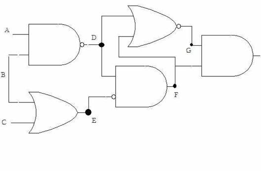
Problem 7
Given the logic
circuit in the figure below, A, B and C are inputs while Z is the output (or see
Figure 3.38 on Page 88 of ItCS).
Draw a truth
table for the output value Z, using intermediate points D, E, F, G to help
evaluate.
Problem 8
a. Draw a transistor-level
diagram for a three-input AND gate and a three-input OR gate. Do this by
extending the designs from Figures
b. Replace
the transistors in your diagrams from part (a) with either a wire or no wire to
reflect the circuit’s operation when the following inputs are applied.
(1) A = 1, B = 0, C = 0
(2) A = 0, B = 0, C = 0
(3) A = 1, B = 1, C = 1