
Third Tutorial
Full-custom Layout Editing
University of Wisconsin, Madison
Spring 1999
In this tutorial you will learn the basics of full custom layout editing by drawing the layout of a simple inverter. As you know, a CMOS inverter consists of a PMOS and an NMOS. The layout has to be as small as possible (to minimize parasitics), and correct, in the sense that the design rules should not be violated. Additionally, you will learn how to create hierarchical cells, and some related concepts.
You will now be guided step-by-step through the drawing of the layout of an inverter. The gate of the PMOS will have a length of 2 lambdas (L=2) and a width of 17 lambdas (Wp=17). The gate of the NMOS transistor will have the same length but the width will be 13 lambdas (Wn=13). You are also provided with the image of the layout of the final inverter.
Run IC Station, by typing ic at the command line. Note that it is very important to see the right colors when drawing layout, so run Netscape after you first run IC station.
You first have to select the Process and the Design Rules that you will use in your layout. From the menu at the top of the screen, select File->Process->Load. In the form that will appear, type $MGC_HEP/technology/ic/scmos and the SCMOS process will be specified. Then, select File->Load Rules, and type $MGC_HEP/technology/ic/scmos.rules in the form that will appear. This loads the corresponding set of Design Rules that we will use in this class. Note that the Process and the Design Rules will be automatically loaded if you have the right startup file (icgraph.startup) in the mgc/startup directory.
Select Cell->Create to create a layout cell. In the form that will appear, give the Cell Name `my_inverter'. The Angle Mode has to be `Ninety'. This means that only horizontal/vertical lines and rectangles can be drawn. The other options need not be changed. Note that the Geometry Editing mode is selected. This means that you are going to do full-custom layout (instead of standard-cells, for example). The form should now be similar to this.
From the menu at the right part of the screen, select Easy Edit.
Select View->Zoom->ToGrid. Each grid space corresponds to half lambda.
From the right part of the screen, select AddObjects->Ruler and click to two points in the layout area. You will see a ruler that is useful in measuring the dimensions of the shapes and paths that you will draw later. You can also measure dimensions with the counters that appear at the top of the IC window.
You will first design the PMOS transistor. Since the length of the transistor will be 2 lambdas and the width 17 lambdas you need to add a poly rectangle with these dimensions. This will be the gate of the transistor. Select AddObjects->Shape. Click on the Options of the menu that will appear at the bottom. You see all the different layers listed . The color and pattern, a code number (GDS II format), and a short description appears for each layer. Notice the correspondence between the code numbers and the CIF names in table 4 of the handout MOSIS Scalable CMOS Design Rules. Select Poly (code 46). Click OK at the above form. Draw a rectangle with length 2 and width 17 (note that in the layout terminology the length of the gate rectangle is normally smaller than the width). Unselect the poly rectangle by pressing F2. It should appear as a red shape now.
You will now add a rectangle that will correspond to the Active region of the transistor (layer 43, CAA). From the design rule 3.4 you know that the active region has to extented by 3 lambdas in each side of the polysilicon. So draw a rectangle with dimensions 8 x 17 centered at the poly. The layout should be like this now.
See design rule 3.3. We have to extend the poly gate 2 more lambdas beyond the active at both ends. The extension can be made easily with the notch command. Select the poly layer (note that only the select layer has to be selected). Click on the notch command at the right of the screen. Draw the extension of the poly layer (you finish the operation by double clicking at the same point). The layout should be like this now.
Note that unselected objects tend to be hatched, and selected objects are only outlines. Sometimes it is difficult to select just one shape. The Select->One command can come in useful. Note that at the bottom of the screen you see the `selection count' which is the number of the objects that you have selected.
If we place a P+ select layer (layer 44, CSP) around the active region we have a PMOS transistor. See the design rules for the select layer (page 10). The select layer rectangle has to extented 2 lambdas beyond the active layer (rule 4.2). Draw it with dimensions: 10 x 19. Actually, for this layout to be a PMOS transistor we also need to draw an N-well around the P+ select (remember that we use an N-well technology which means that the substrate is a P-well). We will add the N-well later, however. The layout should be now like this.
You will now create an NMOS transistor copying the PMOS transistor. Select all your drawing. Then select Edit->Copy. Place the copy below the PMOS transistor. Select the P+ select layer and delete it. Then replace it with an N+ select (layer 45, CSN) of the same dimensions. Notice from the design rules in page 10 that the two select layer may be coincident but they should not overlap.
The NMOS transistor has to be 13 lamdas wide. So you have to reduce the dimensions of the poly, the active and the N+ select layers. Use the Notch command. A few words on this useful command (from the IC Station User's Manual, page 25-52): "If you select a polygon, you can notch-in and notch-out any edge, and the overall area of the polygon changes by the area of the notch that you create. When you notch in, you cut out parts of the selected shapes; when you notch out, you add to each selected object. You can also use "notch" to cut a hole in an object or you can notch through an object to create multiple objects."
Connect the two transistor gates together with a piece of poly. The layout should be now like this.
We now have to connect the two sides of the transistors together (the drains). This node will be the connected to the output of the inverter. The connection will be made using Metal 1 (layer49, CMF) and Contacts to Active (layer 48, CCA). See the design rules at pages 12, and 15. Can you come up with the right sizing of each of the layers? Note that you have to extend the active and the select layers. For the rest of this tutorial you will have to figure out the right dimensions based on the design rules handout. If you want to draw area-efficient layout you will have to use the smallest dimensions that do not violate the design rules.
Extend appropriately the active and the select layers of the two transistors. Draw a metal 1 rectangle above the side that is going to be the drain. This line should extend above both drains. Place one contact to active between metal 1 and the active of the pmos. The more contacts you have the better is the connection (the less the resistance). Do not forget however that contacts need to be placed at a minimum spacing of two lambdas. Copy the contact to the appropriate positions. Notice that for the pmos transistor you can place four contacts while for the nmos three contacts. The layout should be now like this.
Now you will draw the power distribution lines (VDD and GND). You will use Metal 1. The width of the power distribution lines is usually larger than the minimum possible one. The reason is that the resistance of these lines has to be small (the wider the line, the smaller its resistance). Notice that the power distribution lines are usually very long because they have to cover the whole chip area. If their resistance is large there will be significant IR voltage drop along these lines. This means that not all the areas of the chip will "see" the same VDD and GND voltage levels. For this example you will draw the VDD and GND lines with a width of six. The layout should be now like this.
You will now connect the source of the PMOS to the VDD line and the source of the NMOS to the GND line. Use metal 1 for the connections. The width of these lines can be the same with the width of the line that connects the drains (4 lambdas). Place the contact to active as you did before. The layout should be now like this.
As mentioned before, you have to draw an N-well around the PMOS transistor. Notice from the well has to be at least 6 lambdas far from the source/drain active (design rule 2.3). Note that you do not have to draw a P-well because the technology we use is N-well. The layout should be now like this.
Now you will place the substrate contacts. This means that you have to connect the N-well to VDD and the P-substrate (which is something that we do not have to draw; it extends to all the chip) to GND. For the N-well substrate contact you need a N+ select square, an active square, and a contact. They can all have the minimum dimensions. Note that the contact and, if possible, the active, have to be below the metal 1 VDD line to have a better connection. Do the same for the P- substrate contact. In this case you need to have a P+ select square instead. The layout should be now like this.
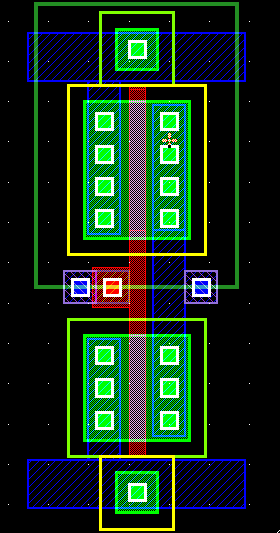
Now you will create the input and output of your inverter. You will use metal 2 for these ports. Note that the output is the drains-connection which is in metal 1. So you need to extend this metal 1 line at the right and draw a `via' square (layer 50, CVA) on top of it. See the design rules 8.1-5 for the right dimensioning. Then draw a Metal 2 (layer 51, CMS) square on top of the via and of the metal 1 layer. See the design rules 9.1-3. Select the metal 2 layer. Draw on top of it one more layer. This will be metal2.port (layer 3). Select Connectivity->Port->MakePort.. At the menu that will appear, specify that it will be an Output Signal with name OUT. The layout should be now like this.
The input is a bit more complex. Since it is a poly connection of the two gates, you have to make a connection from poly to metal 1 and then a connection (via) from metal 1 to metal 2. Notice that the two connections cannot be one above the other. You have to extend the poly layer to the left, add a metal 1 rectangle, add a Poly contact (layer 47, CCP), add a metal 2 rectangle, and then a via. After you do the above, draw on top of the metal 2 rectangle a metal2.port rectangle in the same way you did for output port. This time, you will specify that this will be an Input Signal port with name IN. The layout should be now like this:
Draw the VDD and GND ports using the same procedure. You will use metal1.port (layer 2). This time you will specify that the ports are Power Inputs with names VDD and GND respectively. This completes the port specification of your inverter. The layout should be now like this.
At this point you have to check your layout for any violations of the scmos technology design rules. At the right part of the screen, select Back, ICrules, and then Check. At the menu that will appear press OK. After the checking is complete you can see your layout "bugs" by clicking at "First" for the first error and then at "Next" for subsequent errors. The design rule that is being violated at each case appears at the bottom of the screen. You can return at the editing mode clicking on "Back" and then "EasyEdit". Correct any errors that exist in your layout. If you have a layout design that is free of errors you are done. Note however that a correct layout is not necessarily a good layout. A good layout is one that is:
1. As small as possible (following, of course, any specifications on the transistor lengths, widths, and on the width of the power distribution lines).
2. The parasitics (capacitance and resistance) have to be reduced as much as possible. Note for example that the active regions add to the transistor capacitances, the poly layer is highly resistive, while the number of contacts at a connection has to be the largest possible to reduce the connection resistance.
3. The layout has to have a flexible interface so that it can be connected to other layout pieces or it can be used as a general circuit in various places at your layout.
In large designs, we normally follow a hierarchical layout approach (as opposed to a flat layout approach). Suppose for example that you want to design a buffer using two instances of the 1-bit inverter of the previous section, First, you need to do some additional editing on the 1-bit inverter, so that it is ready for hierarchical layout.
Start by adding a rectangle with the fp1 layer around your inverter. This layer does not correspond to a physical mask layer. It is only used for providing IC Station with information about the boundary of a cell which is mainly used when designing standard cells, which are placed adjacently within rows.

Note that the fp1 outline does not have to include entirely the shapes of a cell. For example, in this case some parts of the N-well are beyond the cell boundaries, since there will be no design-rule violations if N-wells of different instances overlap with each other. In general, we want the cell to be as small as possible, with the constraint though that when cells are placed adjacently there will be no design-rule violations.
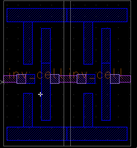
Another important concept when doing hierarchical designs is that of the cell's aspect. The internal aspect of a cell is its complete implementation, with all the including shapes being visible. For example, the previous image shows the internal aspect of the inverter. The external aspect of a cell shows the interface abstraction of a cell, or in other words, what is visible from this cell at the higher-level of hierarchy. It is a good practice to include in the external aspect all the Metal-1 and Metal-2 shapes (including the Port shapes), so that the routing wires at the higher-levels of the hierarchy do no cross the internal metal layers in the cell. For example, the external aspect of the inverter is:

In order to specify that certain shapes are in the external aspect only, or in both the external and in the internal aspects (as in this case), you have to either select them and then change their aspect with the menu Objects -> Change -> Aspect, or to draw them from the beginning in the right aspect, setting the corresponding option in the Add Objects -> Shape menu. You can control the cell aspect that is visible at each time using the menu View -> Show -> Aspect.
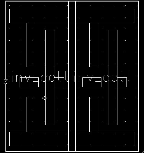
Now, you have to create a cell from the layout of the 1-bit inverter. This cell can be either a block or a standard cell (or several other types of IC Station cells that we ignore for now). First, select all the shapes of the inverter layout. Then, select the menu Objects -> Make -> Cell . In the menu that will appear you have to select the type of the cell and a logical name for the cell. In this case, specify that the cell will be a block (which is what we will be doing in the rest if this course) and give for example the name inv_cell. Then, save the cell using the menu File -> Cell -> Save Cell -> Hierarchy and close it.
Now, create a full-custom cell for the buffer. The buffer will consist of two inverters connected in series. After you create the cell, as you did for the inverter, select Easy Edit and then Add Objects -> Cell. In the menu that will appear, type the logical name of the inverter block that you created before (i.e., inv_cell). Then place the outline that appears somewhere in the buffer's layout. Do the same again for the second inverter. You should now have the following layout (depending on how you placed the two inverters):
You can now add the required interconnects and ports for the buffer. For example, in this case you can use Metal-2 to connect the output of the first inverter to the input of the second.
You can navigate in the hierarchy of a cell using the Peek/Unpeek operations of the Context -> Hierarchy menu. Specifically, you can see at a lower level of a hierarchical cell using the Peek operation, while you can undo this and return to the top level of the hierarchy using the Unpeek operation.
Also, you can change the editing Context in the hierarchical cell, using the Context -> Hierarchy -> Set Context operation. The "context" specifies the cell that you currently edit. For example, if you want to change something in the inverter cell, as opposed to the buffer cell, you can use this operation to specify that you set the context in the "inv_cell" cell. Whatever changes you will do at that cell, however, will automatically be reflected in all the instances of the inverter cell.
Finally, you can flatten a hierarchical cell. This operation should be used carefully, though, and only when necessary, since flat designs are harder to maintain and debug. You can flatten a design by selecting a number of cell instances and then using Othe menu Edit -> Flatten .