$PROJ_PARTS_cs755
/afs/cs.wisc.edu/p/course/cs755-david/public/html/ICstation
Note that you only need to do this part of the tutorial once.
Logic Design
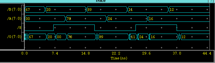
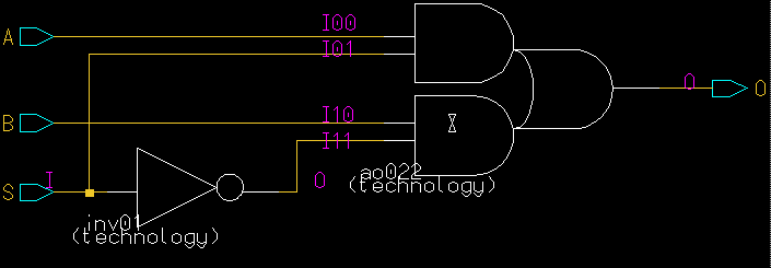
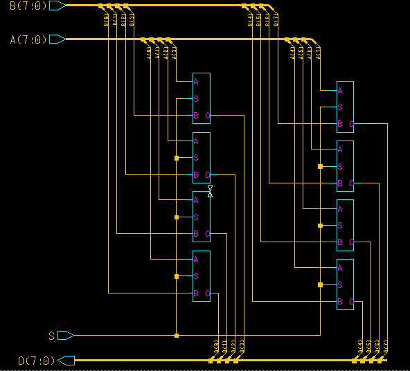
The first step of the process is to design an 8-bit 2-by-1 multiplexer using the scn08hp library of logic components. Note that each of these components corresponds to a standard cell which will be used when you create the layout for this design. The multiplexer will be designed using Design Architect and following the procedure explained in the second tutorial. For example, you can first design a 1-bit 2-by-1 multiplexer, and then use this block in the design of the 8-bit multiplexer. Do not forget to check your design and create a symbol for it (see tutorial-2). It is also recommended that you first simulate your logic design with QuickSim for functional verification, before you try to synthesize the standard cells layout.
Viewpoint Creation
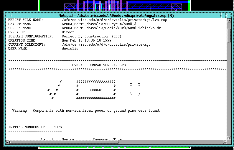
You will now create a viewpoint of the multiplexer for QuickSim, a viewpoint for IC Blocks, and a viewpoint for IC Trace (LVS).
Open DVE by typing dve.
-
First create a viewpoint for the QuickSim digital simulator.
To do this, open a viewpoint for the 8-bit multiplexer component called
qsim_dv_mux8 (or any name you want).
Add an expression primitive called model, and
give it the value technology.
Also add a string parameter
named technology and give it the value scn08hp_nom.
Then, use Setup to set the defaults for QuickSim.
Save and close this viewpoint (without closing DVE).
- Now create a viewpoint of the 8-bit multiplexer component for the IC Blocks place-and-route tool. To do this open another viewpoint called, say, icblocks_dv_mux8. Add an expression primitive called model, and give it the value technology. Also add a string parameter named technology, and give it the value scn08hp_nom. Note that this is just like a QuickSim viewpoint without, however, the setup for the "QuickSim&QuickPath" defaults. Save and close the viewpoint.
-
Now create a viewpoint of the 8-bit multiplexer component
for the IC Trace Layout-Versus-Schematic tool.
To do this open another viewpoint called, say, ictrace_dv_mux8.
Add primitive called element, and
do not give to it any value.
Save and close the viewpoint.
The Three Layout Editing Modes
Placement and routing is the process of automatically generating a layout from a previously existing schematic. To increase our confidence in the correctness of a generated result, we setup IC Graph (the layout editor) to carefully check every action taken by IC Blocks (the placer/router).
There are three layout editing modes in IC Graph. The Geometry Editing, or GE, mode provides the layout technician the greatest flexibility, as it allows unrestricted manual polygon editing. It does not use or maintain any connectivity information from the part schematic, nor does it check for physical design rule errors. A formal schematic of the circuit simply need not exist. In this mode, IC Graph functions strictly as a "dumb" layout editor, and nothing more.
The Connectivity Editing, or CE, mode maintains connectivity data through the editing process, but does nothing to prevent layout errors from occurring. It will give a warning if a layout connection is inconsistent with a connection in the schematic, but it will otherwise allow the edit to occur.
The Correct-By-Construction, or CBC, mode does not allow any editing action to occur that would violate a design rule or contradict a connection in the design's logic schematic. We will use the CBC mode to monitor the results generated by IC Blocks.
AutoFloorplan, AutoPlace and AutoRoute
We will now use IC Blocks to automatically place and route the 8-bit mux design. Note that as you work through this part of the tutorial there are many options that you may choose along the way to layout completion. This exercise will walk you through a relatively simple, direct path to an automatically placed and routed layout. You are encouraged to explore the tool and experiment further as you approach larger layout tasks.
The IC Graph tool is the main entry point in the IC Station environment. To invoke IC Station from the unix command prompt, simply type ic.
-
You first have to select the Process and the Design Rules that will be used in the layout. From the menu at the top of the screen, select File->Process->Load. In the form that will appear, type $MGC_HEP/technology/ic/scmos and the SCMOS process will be specified. Then, select File->Load Rules, and type $MGC_HEP/technology/ic/scmos.rules in the form that will appear. This loads the corresponding set of Design Rules that we will use in this class.
-
Select MGC->LocationMap->SetWorkingDirectory and specify a
working directory for the layout design process. Note that this
process generates multiple report files, and it is usually a good practice
to have a separate directory for each layout design.
-
Select Cell -> Create from the menu on the right hand side of the
screen. A window titled "CREATE CELL" will appear.
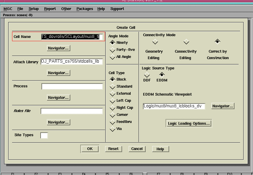
- Cell Name : mux8_layout (a new cell name for the layout)
- Attach Library : $PROJ_PARTS_cs755/stdcells_lib (the standard cells library)
- Angle Mode : Ninety
- Connectivity Mode: CBC (Correct By Construction)
- Logic Source Type : Eddm (schematic in mentor database format)
- Eddm Schematic Viewpoint : icblocks_dv_mux8 (the IC Blocks viewpoint)
- Press the "Logic Loading Options" button. From the pop-up window select Logic Loading: Flat and then press OK.
- Attach Library : $PROJ_PARTS_cs755/stdcells_lib (the standard cells library)
All other options should be left at default values. Press OK and a cell window will appear having the name that you selected. If you do not see a message such as "Logic loading successfully completed. Check the file logic_load.rpt" at the bottom of the window, there is some problem in the mapping of your logic design to layout.
- Cell Name : mux8_layout (a new cell name for the layout)
-
Select Place & Route from the IC Palette at the right menu.
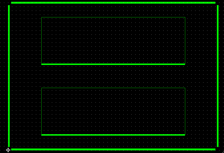
Then choose Autofp , which stands for Auto-Floorplan.
Let all options to default by
clicking OK in the Autofloorplan Options form. Use
View -> All from the top menu bar to see the automatically
generated floorplan. You
will see a series of boxes enclosed by solid bars along each edge.
The boxes indicate the rows into which cells will be organized.
The solid bars indicate edges of the cells along which physical
ports will be placed.
-
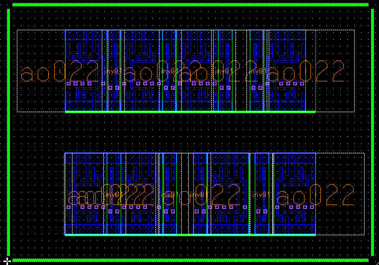
Select Autoplc->StdCel from the Place & Route palette.
Click OK in the form that will appear, once again allowing all options to default.
You will now see the standard cells placed in the floorplan boxes. Cell
locations are determined by their interconnectivity. Cells which share
connections are placed near one another.
You may wish to experiment with the results obtained thus far by selecting
different Autofloorplan and Autoplace options.
It is hard to see clearly each cell's name because they overlap. One
way to see the name for a particular cell is to select it. Since each
"bounding rectangle" overlaps possibly with more cells you have to
press F3 (cycle selection) a few times until the cell that you are interested
in is only selected.
-
Now select Autoplc->Ports from the Place & Route palette.
You can allow the options to default for now, but you may wish to
experiment with them later also. You will see lightly shaded areas
along the port bars at the edge of the layout. By clicking on these
shaded areas you get a message with the name of that particular port.
Alternatively, after you first place the ports automatically,
you can select some of them and place them individually at
the location that you prefer.
-
At this point, it is assumed that you have arrived at a satisfactory
initial placement for all the cells of the layout. Prior to autorouting
the interconnect, you may wish to observe a "rats nest" view of the
signals connecting the various cells. This is sometimes useful to the
layout technician for determining sources of routing congestion.
To observe a rats nest of signal connections, select Connectivity -> Net ->
Restructure -> All signal from the top menu bar. It may look a
little messy, but keep in mind that it doesn't change the layout whatsoever.
-
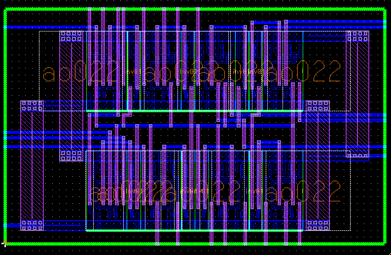
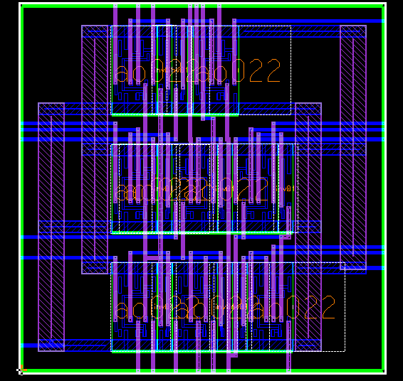
Now select Autorou->All from the Place & Route palette.
Click OK to accept the defaults. This should route all connections
in the mux design. You will see the cell rows move apart and additional
metal runs appear in the channels between rows. Note that one metal layer
(m1) is used largely for horizontal runs and the other (m2) for vertical runs.
By clicking on individual lines you get a message with the name of the net
that corresponds to each line.
-
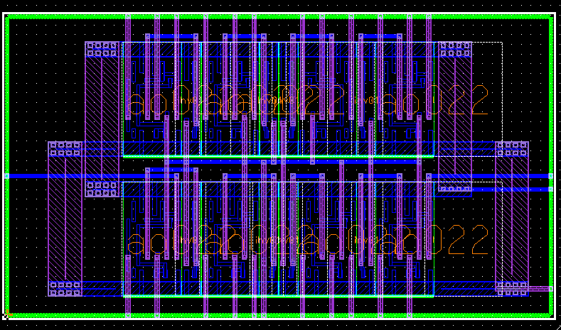
The autorouter's objective is to complete as many connections in the design
as is possible, without regard for wasted area. For this reason,
a layout compactor is available which "squashes" things together where
there is any little bit of unused space. To take advantage of this tool,
select PR Edit->Compct from the Place & Route palette. We
want to compact in both the horizontal and vertical dimensions, so do this
twice: once down and then again in the left direction.
Do not do this more than once along a given axis. Not only
does it rarely result in improvement, it can lead to layout errors
in some versions of the compactor.
- Save the layout by selecting File -> Cell -> Save Cell -> Current Context. You may save the layout and exit the IC Graph session at any time. To re-load the layout later, choose open from the IC Station palette. If you wish to make changes to the cell, you must also select File -> Cell -> Reserve Cell -> Current Context.
At this point, you have completed the automatic layout of your multiplexer. Many options for viewing the results of this process exist. Among these: