DESIGN ARCHITECT
Jack Meador, Madhu Parameswaran and Russ Radke
Washington State University, Pullman WA.
David M. Zar,
Washington University, St. Louis MO.
3-5-96
Minor modifications made by University of Wisconsin, Madison Spring
1999 and 2001
Design Architect is used to enter electronic designs in a graphical
form.
Design Architect is effectively a drawing program that knows
about electrical components, wires, busses and electrical rules. You use
Design
Architect to draw your schematics that you will use later in simulation
or just as a way of neatly documenting your designs.
One way to run Design Architect is from within Design Manager.
From the Design Manager Tools window, double click on the Design
Architect icon (you may have to scroll until you find it). Another
way is to simply enter "da" in response to a shell prompt. The Design
Architect window which appears on your screen should look like that
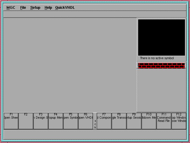
shown in Figure 1.
 .
.
Figure: 1 Design Architect Window
You can fill the screen by clicking on the maximize button on the upper
right corner of the Design Architect window. Once the window is
maximized, you should see a palette of icons on the right side. You can
select these icons instead of going through the menus. These icons will
change depending on the context of your operations, as you will shortly
see.
Before entering your design, it helps to first consider all the different
parts of a schematic inside the Design Architect window. These are
summarized in Figure 2.
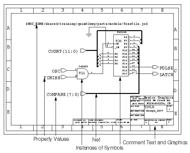
Figure: 2 Elements of a Schematic (Source: "Getting Started with
Design Architect" training workbook.)
All Design Architect schematics contain symbol instances,
nets,
properties,
pins
and ports. Comment text and graphics are often included as well.
Every class of component has associated with it a symbol that is
invoked in the schematic wherever a specific instance of that component
is to be used. Every unique component in a design has associated with it
a symbol instance which is a component symbol at a specific schematic
location. A net is a wiring connection between components. Each
symbol
has associated pins representing external connections to the component.
If the underlying model for a part is also a schematic, every pin
on the part symbol corresponds to a port inside the schematic for
that part.
Symbol pins are connected to each other by drawing nets
between them. Any element of a schematic, such as
symbol instances,
nets,
pins and ports can have associated properties which
give additional information about the element. Properties are described
in terms of a
name,
type, and value. In Figure 2,
the property value FINISH is associated with an input
port
connected via a net to symbol instance U11.
You will now be guided step-by-step through a the process of schematic
capture using Design Architect. The design that you will enter is
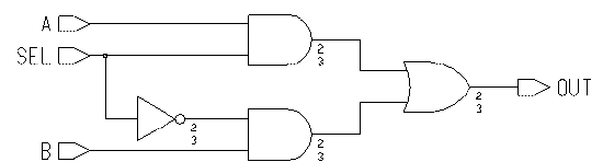
a simple 2-1 multiplexor circuit shown below in Figure 3.
 .
.
Figure 3: 2-1 MUX Circuit.
Before you begin, make sure that you have created a directory called
mgc/tutorial/schematics
in your private directory. Enter this circuit as follows:
-
Invoke Design Architect with the line % adk_da &
-
Whenever you first begin a Design Architect session, make sure you are
working in the directory you intend to use as the root directory for your
design. Select MGC -> Location Map -> Set Working Directory: from
the top menu bar and either verify or change the entry in the dialog box
which appears. Set it to .../tutorial/schematics
-
Click on the OPEN SHEET icon or select File -> Open -> Sheet
from the menu bar.
-
A dialog box will appear. You should click in the Component Name
box. Now, append /mux21 to the path in the Component Name
box to create a component called ``mux21.'' When you're done, click on
OK.
Actually, you can just type ``mux21'' and don't need the path that's displayed
unless you want to put your design in a different directory.
-
You will see an empty sheet in the Design Architect window into
which you can now place components. Click on the maximize button of the
sheet window to give yourself the largest working area possible. To begin,
you need to select a library of components to use. Do this by selecting
CHOOSE
SYMBOL from the schematic add/route palette or, by holding down the
right mouse button to obtain the add menu and selecting Instance ->
Choose Synbol. There is typically more than one way to accomplish something
in Design Architect. This example illustrates two of them: clicking
on a palette icon or holding down the right mouse button to get a context-sensitive
menu. There is also a way to do this via the top menu bar, but it is more
difficult to find. See if you can find it. This will activate a dialog
box which contains a button having four arrows on it, among others. Click
on this button, enter $ADK into the form, then click on OK.
-
Note how the dialog box shows several directories, including one called
``parts''. When you double click on that directory, you will descend into
it and find a list of all parts which are available in this library. Highlight
the and02 part by clicking on it once then click on the ok
button. This will make the and02 our current active part.
-
Now, move the pointer into the schematic sheet. The gate will appear, and
you can drag it to the position where you want to place it. To place the
gate symbol, click on the point where you want it to be.
-
Next, place the other and02 gate in the same way: click on the gate's
icon in the active symbol window at the upper right corner. Drag
and place it on the schematic. Be sure to leave space between the components.
Do not overlap the components or you will not be able to simulate the schematic
later.
-
If you need more drawing space for your schematic, first be sure the drawing
window is maximized. If it is, you can zoom out by using the right mouse
button to display the pop-up menu. Select the Zoom submenu and
then select the direction (in or out). Zooming out displays more area,
and zooming in displays less.
-
Place the OR and INVERTER gates in the same way, by clicking and dragging.
Use or02 and inv02 from the palette.
-
Now place the port connections (A, B, SEL, OUT) by referring to the symbol
history in the active symbol window menu. Move the mouse pointer to
the active symbol window, and hold down the right mouse button. At this
point, your screen should look something like this.
Select symbol history to obtain the portin and portout
symbols. The ``portin'' symbol is used for inputs and the ``portout'' is
used for outputs. Place the appropriate symbols on the schematic sheet
as shown in Figure 3.
-
Next, you need to wire up the components. Note how the bottom of your screen
has function key labels on it, and that F3 is labeled as Add
Wire. One way to start wiring is by hitting the
F3 key. Another
is by clicking on the ADD WIRE icon in the schematic_add_route palette.
To make it easier to access this icon, you may have to resize that palette
and add scroll bars. You may use the palette menu accessed by holding down
the right mouse button over the palette to do this if you wish.
-
You wire between two points by clicking on the starting point and double
clicking on the ending point. If you want to put a bend in the wire,
just click once at the point where you want to bend the wire. Place the
wires as shown in Figure 3.
-
When you're done wiring, click on the Cancel button on the dialog
box at the bottom of the screen. Your screen should now look something
like this.
-
Note how the schematic now has different values displayed in various places.
Each logic gate has pin properties attached to all of its inputs and outputs.
Pin properties are strings given the values "I0" and "I1" for inputs and
"O" for the outputs with the gates you have used. Every wire you have drawn
also has a string property called "NET" which is assigned the default initial
value "NET". We will change this value where we need to explicitly label
wires. Finally, you'll see how there is associated with every logic gate
an expression property called "MODEL" which has the value "(technology)".
-
We will now modify those property values which we expect to never change
throughout the design process (such as "NET" property names). They will
become a permanent part of the schematic. Properties which we expect to
change at times throughout the design process (such as the "MODEL" property)
will be changed using schematic viewpoints instead of maintaining different
versions of the schematic. But first, before continuing, unselect everything
by using function key F2.
-
There are many ways of selecting objects in a schematic. For simpler tasks,
perhaps the easiest way to do so is simply by moving the cursor over the
item you wish to select and hitting the F1 key. Another way is to
drag the left mouse button over an area of the schematic which will select
all objects inside the box and which cross its boundaries. An elaborate
selection filter exists for specifying the selection of just specific things
inside the selection area (see the SET SELECT FILTER in the schematic_text
palette). For now, our task is simple, so we will use the first method.
-
Select all of the NET property values using the F1 key. Make
sure that these are the only things you select. You can keep track in two
ways. First, selected items turn white. Second, you can watch the selection
counter in the top status bar of the screen. After completing your selection
process here, this should read Sel: 4+ because you have selected
exactly four things. If you accidently select wrong things, use UNSELECT
ALL in the palette or the F2 key.
-
Next, choose the TEXT icon in the schematic palette. This will cause
the palette to change to the schematic text palette. From this new palette,
select CHANGE VALUE.
-
A dialog box will appear at the bottom of the screen. Notice how the value
you are currently changing remains highlighted in the schematic so you
know which one you are changing. Simply type the correct new value over
the old and hit the return key. In the case of NET, you should
change its value to the desired wire label as shown in Figure 3. When the
last name is changed, the prompt bar disappears. It is very important that
you change property value only. Do not change anything else in the
dialog boxes which appear.
-
You must now check the drawing before you can save it and take a break.
If your sheet does not pass this check, you cannot simulate it (of course,
you are not allowed to take the break until it passes!). To check your
sheet, select Check -> Sheet -> With Defaults from the menu bar.
There should be no errors. Sheet errors are often caused by drawing errors
(such as having two outputs connected together) and many are quite self-explanatory.
When errors and warnings are present, just click on the text in the report
form, and the offending portion of the schematic will become highlighted
(if it's visible). A simple example of an inconsequential warning is shown
here.
This one is fixed by eliminating the overlap between the property text
and the port B symbol. Even though warnings may not keep your simulation
from running, you should still try to eliminate them. Once that warning
is eliminated, the sheet check results should look something like this.
Even with a perfectly drawn schematic, you should still notice instance
warnings at this stage of the design when using the ADK library. These
warnings arise from the variable properties we have chosen to establish
in a separate schematic viewpoint. Since we know that we plan to establish
these values later, we can ignore the warnings for now.
-
Close the report window by double clicking the upper left window control.
-
Your schematic sheet should now look something like this.
Save it by selecting File->Save Sheet from the menu bar.
-
Any significant digital design requires that some hierarchical organization
be established. To be able to use the 2:1 mux as part of some larger circuit,
it is necessary to have a symbol for it which can be used in higher level
schematics the same way it's schematic references the and02 and
or02
for example. The final step of designing your 2:1 mux will involve the
specification of a symbol which describes how it will interface into larger
systems.
-
From the top menu bar, select Miscellaneous -> Generate Symbol.
A dialog box will appear that gives a variety of options for the automatic
creation of a symbol which encapsulates your logic diagram. The only option
you should need to change is the "Once generated..." column where you should
click on "Save then Edit". If you wish to replace an existing symbol for
this component, then you will also want to say "Yes" to "Replace existing?".
-
Once symbol generation is complete, a symbol editor window is opened which
displays the symbol that was generated. You may now edit the symbol as
you see fit using symbol editor commands. One useful and simple thing to
do is to give the part a name. Do this by selecting the body of the symbol
(the box in this case) and clicking on the add text icon in the symbol_text
palette. A small dialog box will appear where you can enter a name to be
attached like "mux21". When you hit OK, the new text will appear wherever
you wish to place it near or on the symbol. Once this change is made, check
it using Check -> With Defaults from the top menu bar. Then save
and register the symbol with the part database entry by selecting File
-> Save Symbol -> Default Registration. You are done and may close
the symbol editor window when there are no errors, ignore the symbol not
on interface warnings. The mux part can now be incorporated into other
schematics the same way you have just used the ADK library parts.
-
Now you will create a second sheet. In this sheet you will use the
Mux21 sysmbol that you just generated to create a 4-1 mux. Open a
new sheet Session_palette Open Sheet button. Set the component
name to .../schematic/mux41.
-
Select the Choose Symbol button and hit the four arrows button
to select the directory containing the mux21 symbol. Select the mux21symbol
and hit OK.
-
Using the mux21, create a schematic that looks like
this. Make sure to check it, ignore the symbol not on interface
warnings, and then save it.
-
Now create a "mux41" symbol just like you did with the "mux21". Rememeber
to check it and save it.
-
Exit Design Architect by closing the window and responding to the
dialog boxes that appear. You must use the close command from your windows
manager since there is no "quit" function in the menu bar.
You have now completed the schematic capture of the MUX circuit. Soon,
you will be ready to simulate the circuit to see if it is functionally
correct and if it meets some timing constraints using QuickSim II,
the logic level simulator. But first, you must create a special view of
the schematic that will tell QuickSim how to use the MOSIS scn08hp
standard cell library.
Now we are ready to move on to the QuickSim tutorial.