Netlist Extraction from Layout, Backannotation from Layout,
and Accusim Simulations
Constantinos Dovrolis
University of Wisconsin, Madison
Spring 1999.
In this tutorial you will learn how to extract the netlist from a layout cell, and then simulate it with Accusim. Also, you will learn how to backannotate a transistor schematic with the parasitic capacitances from the layout that corresponds to this schematic, and then simulate it with Accusim. These procedures have several variations. For example, the netlist extraction can be performed including only capacitive parasitics, or both resistive and capacitive parasitics. The parasitic models can be lumped or distributed. The netlist extraction can be done in either a "flat", or in a "hierarchical" manner. Also, the simulation of the netlist can be done with Accusim, which is an analog simulator, or with Lsim, which is a semi-digital-analog simulator. The following sections describe only one of these approaches; other approaches may be added to this tutorial in the future.
Suppose that you have created a layout cell with IC Station and you want to verify its correctness. First, you need to run IC Rules in order to check that the cell has no Design-Rule violations. Then, if you designed the cell in Connectivity-Editing or Correct-By-Construction mode, you can check that the layout passes the LVS checks using IC Trace. After you pass these two first tests, you can extract the netlist from the layout and simulate it. This step will prove that the layout is correct (if your test vectors are adequate), and it will also provide you with important timing information.
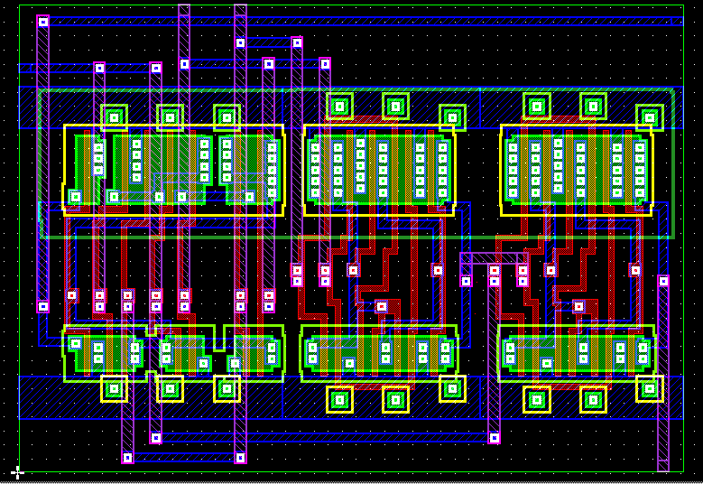
For example, suppose that you have designed the following layout for a full-adder cell (called full_adder.1). Note that this layout is not particularly good because it is not compact (since it was originally designed using standard cells). You can do much better than this if you follow a full-custom approach. The internal aspect of the cell is:

while the external aspect is:

There are several things to note at this point. Make sure that you also follow these steps in your designs:
Now, select the IC Extract(M) menu in order to do the netlist extraction. For a lumped modeling of the layout parasitics, which is adequate for relatively small cells, select the Lumped menu. At the form that will appear select "Yes" at the Netlist button, and then enter a name for the netlist file. For example, the netlist name in this case will be full-adder.1.sp. Also, enter GND as the Ground name. Note that the produced netlist is by default in the HSPICE format. Click OK and the produced netlist will be saved in your Working Directory.
Take a look at the netlist. The first line is a comment. Then, you can see a subcircuit definition:
.subckt full_adder.1 A B CIN COUT GND SUM VDD
The name of the subcircuit (full_adder.1) is the same with the name of the layout cell. The list of the cell ports follows (including VDD and GND). This subcircuit statement defines the interface of the layout cell.
In the body of the subcircuit you can see a long list of device descriptions for the transistors that make up the cell. Each transistor description includes:
Then, you can see the list of parasitic capacitances that are included in the subcircuit. Note that some of these capacitances are between a certain interconnection and the ground, while some others refer to two different interconnections (coupling capacitances). Also note that for such small layout cells, there are normally no extracted resistances. For longer interconnections you will normally, however, see also some resistive parasitics.
At this point we are done with the extraction process and with IC Station. The next step will be to simulate this netlist with Accusim. But first, we need to map the netlist to a logic symbol with Design Architect.
We now have to create a logic symbol that will be mapped to the subcircuit that has been extracted from the layout.
Run Design Architect. Select Open Symbol, and specify a name for the logic symbol (e.g., full_adder.1). Now, use the Add Rectangle and Add Pin buttons, in order to draw something like the following:
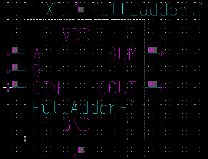
Specifically, do the following:
Now, we have to create a schematic for the circuit that will be simulated with Accusim. Use Design Architect again in order to create a schematic, i.e., select Open Sheet. Then instantiate the logic symbol that you created in the previous step (full_adder.1), and draw a schematic such as the following:
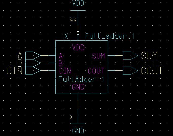
You can find the ports, VDD, and GND symbols from the $MGC_GENLIB library. Remember, though, to specify that the VDD voltage is 3.3 Volts instead of 5.0 Volts. Also, for the GND symbol you can use the Vss symbol, after you rename it to GND and then you assign to it the value of 0 Volts. After you are done with this editing, Check, Save, and Close this schematic.
Note that the logic diagram that we created at this step does not have to be mapped in such a simplistic way to the extracted netlist. In fact, this schematic corresponds to what we want to simulate with Accusim, and not to what we extracted from the layout with IC Extract. Consequently, it can include several different symbols, each of them mapped to the same or to different layout-extracted subcircuits. Also, some of the symbols in this schematic can be mapped to a transistor-design (see Tutorial-5), instead of being mapped to a layout-extracted subcircuit.
NOTE: It seems that Accusim does not like busses and signal names that are `bus-like' (e.g. A(1), A(2), etc). If your design includes busses, use individual signals instead, and instead of giving the signal names in parenthesis, use something like A_1, A_2, etc.
Now, run the Design Viewpoint Editor (DVE). Open a viewpoint, named for example full_adder.1.dv, and select Setup -> Accusim. This step creates an Accusim viewpoint for the logic design that we just designed. Save the viewpoint, and close DVE.
You are (finally!) ready for the Accusim simulation. From the Design Manager tools window, run Accusim. In the form that will appear, use the navigator to select the design viewpoint that you created in the last step. Click OK, and the Accusim window will pop up after a while.
After this point, the simulation procedure is basically the same with any Accusim simulation (see Tutorial-5). Before we are ready to run the simulation, however, we need to do the following steps:
X_I$8 COUT SUM A B CIN 0 VDD full_adder.1
Note the order with which the ports of the full_adder appear. Now, manually edit the netlist file (full_adder.1.sp) so that the ports appear these in the same order, i.e., after the editing that netlist line should be:
.subckt full_adder.1 COUT SUM A B CIN GND VDD
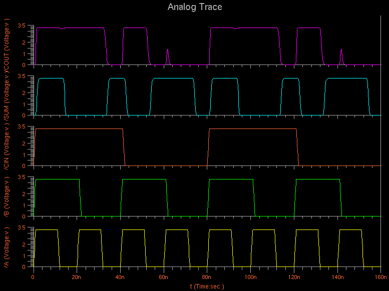
Now you can setup Accusim for a Transient simulation, setup the traces, apply some forces, and run the simulations. For example, the following traces resulted for this full-adder circuit:
Note that Accusim offers several different simulation parameters and algorithms. If you are simulating a large circuit which takes too long to simulate, you may have to use a less accurate but faster simulation setup. In that case, let the TA know as soon as possible.
So far, you saw how you can do such simulations using Netlist Extraction. This procedure is quite lengthy and error-prone. There is, though, an alternative for doing post-layout verification using Accusim, that is based on backannotation. You may want to use either extraction or backannotation, or both. In general, the extraction method is more reliable and accurate, since the simulation is based on the actual extracted information from the layout. Additionally, the netlist contains some additional geometrical information about the devices (source and drain areas), that is not included in the backannotation. Also, the backannotation does not include coupling capacitances, but only capacitances between each node and GND. On the other hand, backannotation-based simulations are easier to make.
Specifically, suppose that you have a Design Architect transistor-based schematic. Also, you have created an SDL viewpoint for this schematic (using the sdl_prep) script. Suppose now that you are done with the creation of the layout (using full-custom or SDL), and that you have run DRC and LVS successfully. Now, select IC Extract (M) and then Lumped, as you would normally do for extracting a netlist. In the form that appears, however, do not select "Netlist", but "Specify Schematic Source". As the "Source Name", type the path of the SDl viewpoint that you created with sdl_prep. For example, type something like:
$PROJ_PARTS_youraccount/MyDesigns/CSA_19bit/sdl
Then, select "Setup LVS", and do whatever you would normally do when running an LVS check (select GND as the ground name, and specify that the tool should not try to recognize gates).
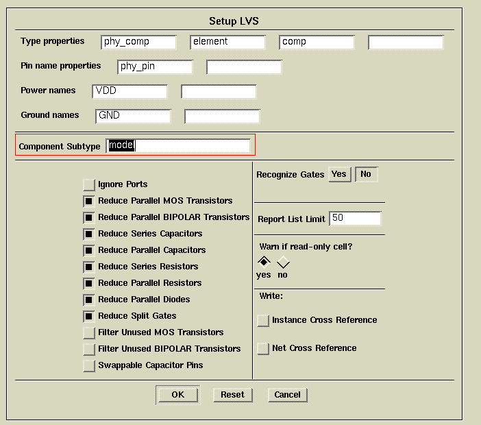
Also, select "Yes" in the "Backannotate" option, and then specify a "BA Name" for the backannotation (e.g., CSA_19bit.ba). Finally, as the "Lumped Capacitance" property name, select cap_net, as opposed to icap_net.
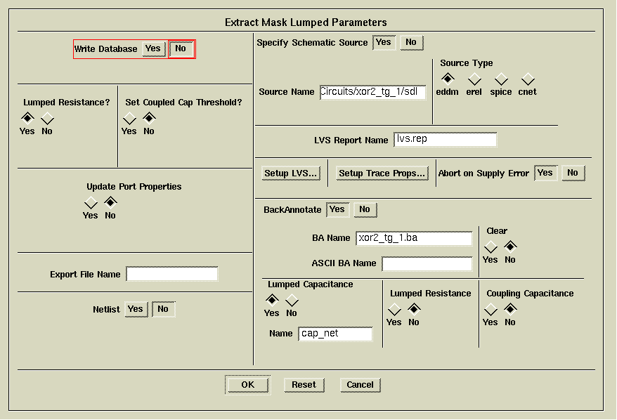
Click OK, and the backannotation will be created and attached to your SDL viewpoint. If you want to see the actual capacitance values, open the viewpoint with DVE. For each wire that you select, you can view (and edit) the parasitic capacitance by editing the property "cap net" of the wire. Note that reported values are in picoFarads.
Now that you have the backannotated SDL viewpoint, you can simulate it with Accusim as you know from tutorial-5. Two important points, though: