|
Homework 3 // Due at lecture Wed, Feb 16
Primary contact for this homework: Peter Ohmann [ohmann at cs dot wisc dot edu]
You may do this homework with one other person from your section.
You must put both names on the assignment. Please staple multiple pages together.
Problem 1 (2 points)
Draw a transistor-level circuit for a three-input AND gate.
Note: The following is not the only possible answer:
Problem 2 (3 points)
-
Draw the gate-level representation for an eight-input multiplexer.
-
If you were to draw a 32-input multiplexer, how many select lines would be
required?
5 (32 = 25)
Problem 3 (3 points)
-
Draw a gate-level circuit for the following logic expression. Do not simplify the
expression. Your circuit must use 3 AND, 2 OR, and 2 NOR gates.
Z = ((A AND B) OR (C AND D)) OR (NOT(A OR B) AND NOT(C OR D))
-
Find the truth table for this circuit.
| A | B | C | D | Z |
| 0 | 0 | 0 | 0 | 1 |
| 0 | 0 | 0 | 1 | 0 |
| 0 | 0 | 1 | 0 | 0 |
| 0 | 0 | 1 | 1 | 1 |
| 0 | 1 | 0 | 0 | 0 |
| 0 | 1 | 0 | 1 | 0 |
| 0 | 1 | 1 | 0 | 0 |
| 0 | 1 | 1 | 1 | 1 |
| 1 | 0 | 0 | 0 | 0 |
| 1 | 0 | 0 | 1 | 0 |
| 1 | 0 | 1 | 0 | 0 |
| 1 | 0 | 1 | 1 | 1 |
| 1 | 1 | 0 | 0 | 1 |
| 1 | 1 | 0 | 1 | 1 |
| 1 | 1 | 1 | 0 | 1 |
| 1 | 1 | 1 | 1 | 1 |
Problem 4 (5 points)
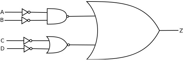
Given the circuit:

-
Draw the truth table.
| A | B | C | D | Z |
| 0 | 0 | 0 | 0 | 0 |
| 0 | 0 | 0 | 1 | 0 |
| 0 | 0 | 1 | 0 | 0 |
| 0 | 0 | 1 | 1 | 1 |
| 0 | 1 | 0 | 0 | 1 |
| 0 | 1 | 0 | 1 | 1 |
| 0 | 1 | 1 | 0 | 1 |
| 0 | 1 | 1 | 1 | 1 |
| 1 | 0 | 0 | 0 | 1 |
| 1 | 0 | 0 | 1 | 1 |
| 1 | 0 | 1 | 0 | 1 |
| 1 | 0 | 1 | 1 | 1 |
| 1 | 1 | 0 | 0 | 1 |
| 1 | 1 | 0 | 1 | 1 |
| 1 | 1 | 1 | 0 | 1 |
| 1 | 1 | 1 | 1 | 1 |
-
Write the (unsimplified) logic expression.
(NOT(A) NAND NOT(B)) OR (NOT(C) NOR NOT(D))
-
Simplify the expression and redraw the circuit.
A OR B OR (C AND D)
-
What principle (from the textbook) does this demonstrate?
DeMorgan's Law
Problem 5 (3 points)
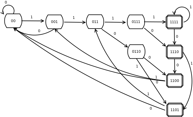
Draw the FSM state-diagram for recognizing all 4-bit unsigned numbers greater than
or equal to 12. (Hint: Each edge will either correspond to
a 1 or a 0. If the last four bits correspond to a value greater than or equal
to 12, your FSM should have 1 as output; otherwise, it should have 0). For
help, look at the lock example in Figure 3.28 of the textbook (this is an
extension of that example).
Note: The following FSM would apply for extra credit. The
standard version would be much simpler, with only 4 states after the start
state (one for each bit read).
Note: The double-circle states are [out=1] states. Single circles indicate
[out=0].
Problem 6 (3 points)
How many memory locations can be addressed with a 16-bit address? Assuming the
memory is byte-addressable and we are working with standard 32-bit integers,
what is the theoretical maximum number of integers we could store and reference
in our memory? (Hint: Think about how many total bytes/bits are in the memory).
You may, of course, provide your answers as 2n.
216
216 / 22(32 bits = 4 bytes = 22) =
214
Problem 7 (4 points)
The figure below shows the gate-level circuit for a half-subtractor and its
associated truth table. Similar to the full-adder, the full-subtractor takes
two bits to be subtracted and a borrow-in, and outputs the result bit, and a
borrow-out. Based on this and your knowledge of the full-adder:

| X | Y | D (difference) | Bout (borrow-out) |
| 0 | 0 | 0 | 0 |
| 0 | 1 | 1 | 1 |
| 1 | 0 | 1 | 0 |
| 1 | 1 | 0 | 0 |
-
Draw the truth table for a full-subtractor. Use columns X, Y, Bin,
D, and Bout.
| X | Y | Bin | D | Bout |
| 0 | 0 | 0 | 0 | 0 |
| 0 | 0 | 1 | 1 | 1 |
| 0 | 1 | 0 | 1 | 1 |
| 0 | 1 | 1 | 0 | 1 |
| 1 | 0 | 0 | 1 | 0 |
| 1 | 0 | 1 | 0 | 0 |
| 1 | 1 | 0 | 0 | 0 |
| 1 | 1 | 1 | 1 | 1 |
-
Draw the gate-level circuit for the full-subtractor.
This very creative answer came on a number of your homeworks. I hadn't thought
to do it this way...but it works!
Problem 8 (2 points)
If one begins with the R-S latch (Figure 3.18 in the textbook) and replaces
the NAND gates with NOR gates, one obtains what is called an S-R latch.
What impact will this have on the action of the latch?
Note: Your answer should include 2 changes.
1. The "steady" or "stable" state is 0,0 instead of 1,1
2. Depending upon which way you observe it, either the R and S are flipped, or
the output moves from the top to the bottom gate.
|