by
Constantinos Dovrolis
dovrolis@cs.wisc.edu
Monday, February 15 1999.
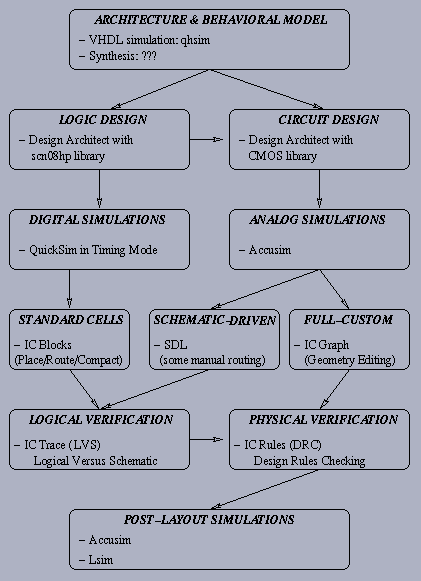
The Overall Picture
The objective in this course is to cover the entire design process, starting from the architecture of a system down to the physically verified VLSI layout. The toolset consists of about ten Mentor Design tools that are briefly covered with on-line Tutorials.
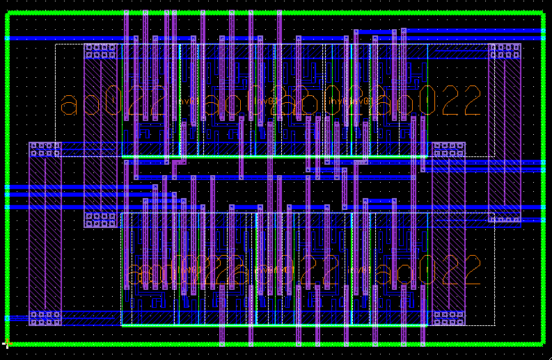
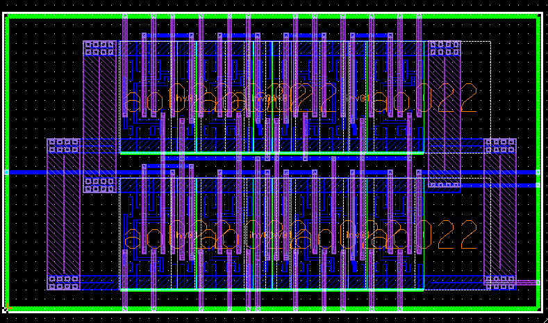
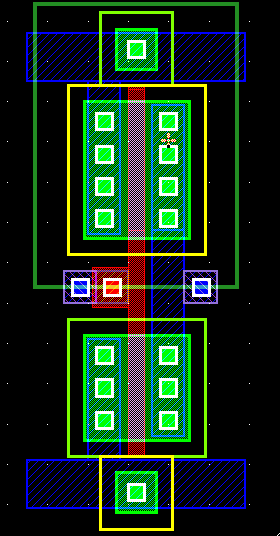
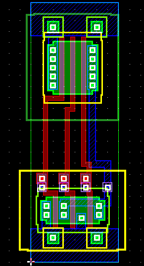
Some Layout Examples
A CMOS inverter
A 3-input NOR gate
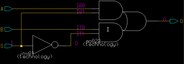
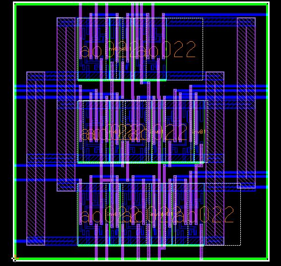
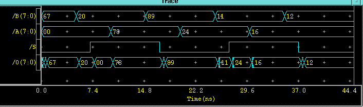
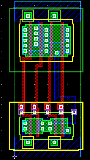
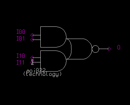
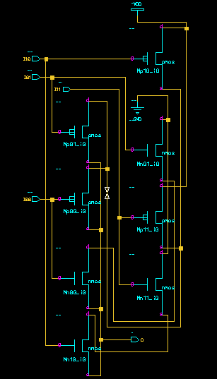
What is the following?
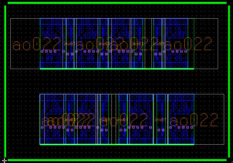
Standard Cells Methodology
A few words about the scn08hp library of standard cells: