Figure 1
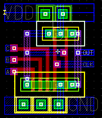
Figure 2
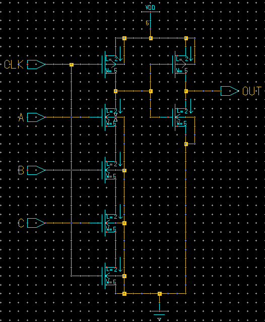
1) Figure 1 and 2 show the schematic and layout for a 3 input
AND gate using domino logic.
|
Figure 1 |
Figure 2 |
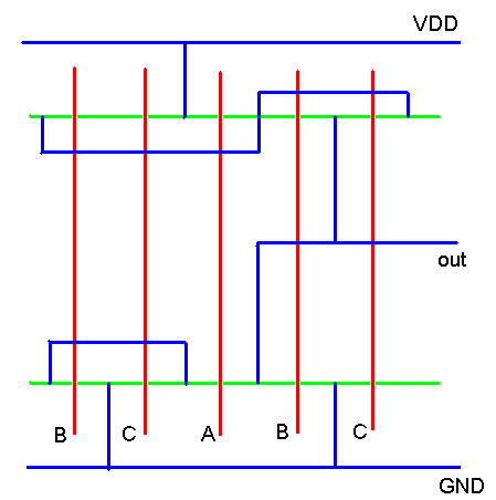
2) Figure 3 and 4 show the schematic and stick diagram for the
F = (AB + AC + BC)'
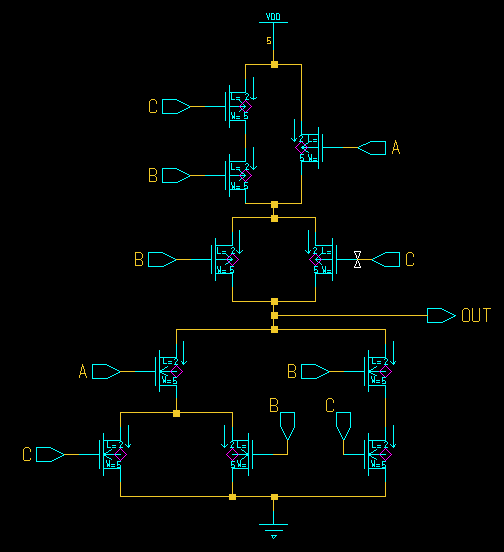
Figure 3 |
|
3)
a) When designing a buffer there are 2 parameters that have to decided - Number of stages and scaling factor. An optimal scaling factor is found to be 2.7 and the number of stages if given by
N +1 = ln(Cload/Cg) / ln(a)
where,
N - number of stages
Cg - Gate capacitance of the input
stage.
Cload - Load capacitance
a - Scaling factor
Since the gate capacitance is not given we take a = 3 and number of stages = 4.
Figure 5 show the design of the
buffer that gives equal rise and fall times. We have a rise time
of 616ps and a fall time of 606ps. The overall delay is given by
(tPLH + tPLH)/2 = 860ps. The rise time, fall time
and the delay calculation are shown in Figures 6,7,8, and 9
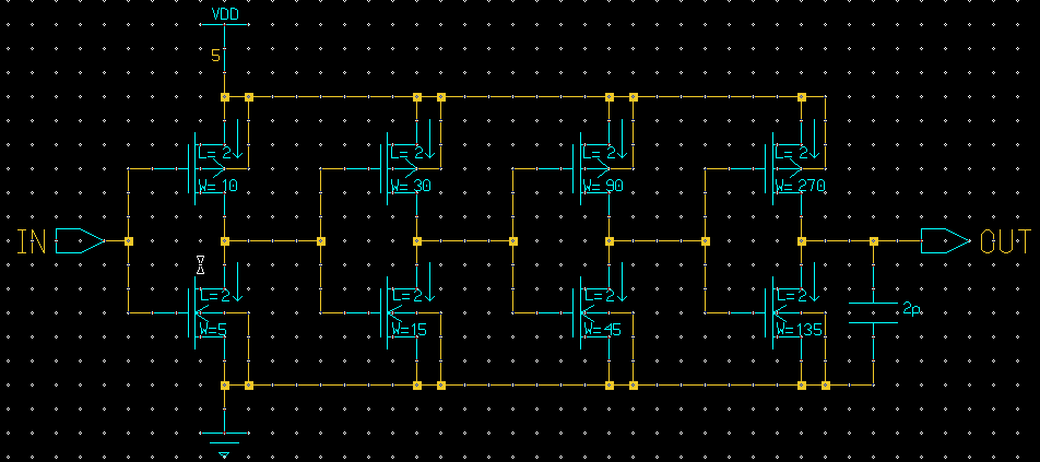
Figure 5 |
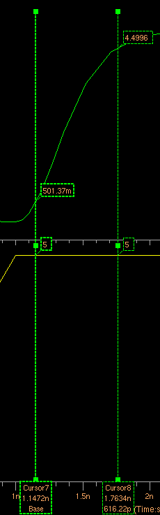
Figure 6 (rise time) |

Figure 7 (Fall time) |
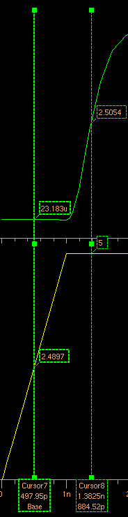
Figure 8 (tPLH) |
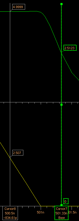
Figure 9 (tPHL) |
From figure 10 and Figure 11 we can calculate the noise margin.
NMH = VOH - VIH = 4.34 - 2.94 = 1.4V > 10% VDD
NML = VIL - VOL = 1.92
- 0.65 = 1.27V > 10%VDD
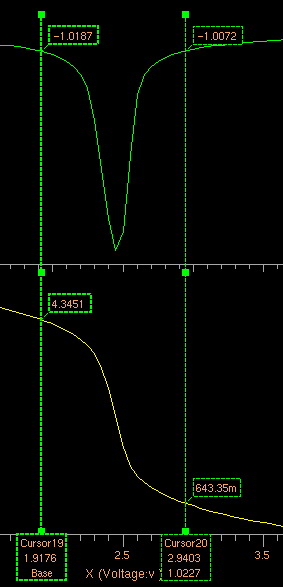
Figure 10 (VTC of 3rd stage) |
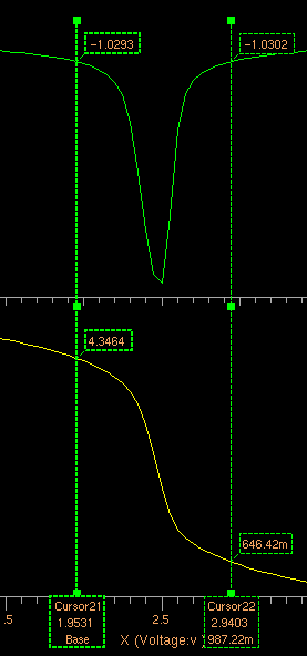
Figure 11 (VTC of final stage) |
b) In order to
minimize the rise time we increase the W/L ratio of PFET. The optimized
buffer design is shown in figure 12.
From figure 13 we can see that the rise time has decreased to 339ps.
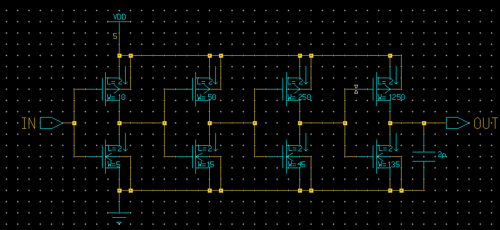
Figure 12 |
From figures 14 and 15 we
can calculate the noise margin to be NMH = 0.68V and
NML = 2.57V.
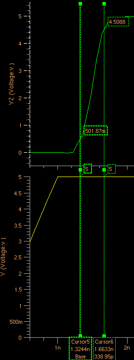
Figure 13 (Rise time of optimized buffer) |
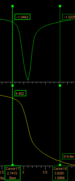
Figure 14 (VTC of 3rd stage of optimized buffer) |
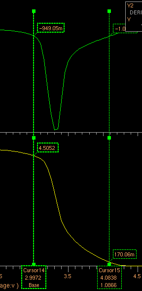
Figure 15 (VTC of final stage of optimized buffer) |
c) From the results
obtained in (a) and (b) we can see that as we increased our rise time we
lost on the noise margin. We got a high noise margin which is well below
20% VDD in (b). Hence having a larger noise margin say above 20% VDD does
affect our design.