AUTOMATIC LAYOUT
Viewpoints
This tutorial requires the creation of the following viewpoints:
- a viewpoint of your 8-bit multiplexer component for QuicksimII
using the script:
~cs755-1/public/html/mentor/qsim_prep
This will create a viewpoint called qsim.vp.
- another viewpoint of the 8-bit multiplexer component for the
IC Blocks place-and-route tool using the script:
~cs755-1/public/html/mentor/auto_prep
This will create a viewpoint called auto.vp.
- and still another viewpoint of the 8-bit multiplexer component
for the IC Trace Layout-Versus-Schematic tool using the script:
~cs755-1/public/html/mentor/lvs_prep
This will create a viewpoint called lvs.vp.
AutoFloorplan, AutoPlace and AutoRoute
We will now use IC Blocks to automatically place and route the 8-bit
mux design. Note that as you work through this part of the tutorial
there are many options that you may choose along the way to layout
completion. This exercise will walk you through a relatively simple,
direct path to an automatically placed and routed layout. You are
encouraged to explore the tool and experiment further as you approach
larger layout tasks.
The IC Graph tool is the main entry point in the IC Station environment.
To invoke IC Station from the unix command prompt, simply type ic.
-
You first have to select the Process and the Design Rules
that will be used in the layout. From the menu at the top of the screen,
select File->Process->Load. In the form that will appear, type
$MGC_HEP/technology/ic/scmos and the SCMOS process will be
specified. Then, select File->Load Rules, and type
$MGC_HEP/technology/ic/scmos.rules in the form that will appear.
This loads the corresponding set of Design Rules that we will use in this
class.
-
Select MGC->LocationMap->SetWorkingDirectory and specify a
working directory for the layout design process. Note that this
process generates multiple report files, and it is usually a good practice
to have a separate directory for each layout design.
-
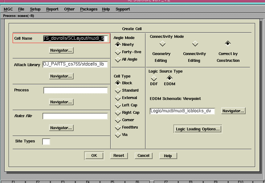
Select Cell -> Create from the menu on the right hand side of
the screen. A window titled "CREATE CELL" will appear.
Enter the following and then click OK:
- Cell Name : mux8_layout (a new cell name for the layout)
- Attach Library : $PROJ_PARTS_cs755/stdcells_lib (the standard cells library)
- Angle Mode : Ninety
- Connectivity?: With connectivity
- Logic Source Type : Eddm (schematic in mentor database format)
- Eddm Schematic Viewpoint : auto.vp (the IC Blocks viewpoint)
- Press the "Logic Loading Options" button. From the pop-up window
select Logic Loading: Flat and then press OK.
All other options should be left at default values. Press OK
and a cell window will appear having the name that you selected. If
you do not see a message such as "Logic loading successfully
completed. Check the file logic_load.rpt" at the bottom of the window,
there is some problem in the mapping of your logic design to layout.
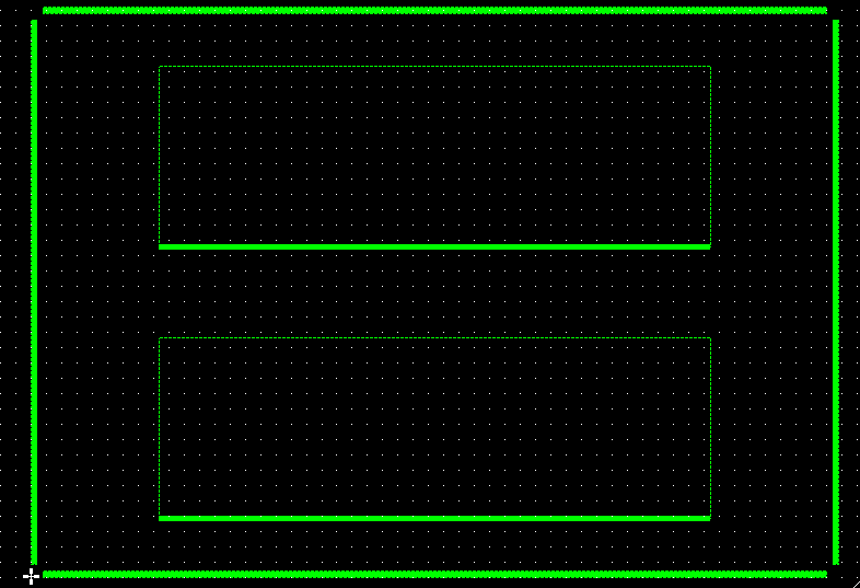
- Select Place & Route from the IC Palette at the right
menu. Then choose Autofp , which stands for Auto-Floorplan.
Let all options to default by clicking OK in the Autofloorplan Options
form. Use View -> All from the top menu bar to see the
automatically generated floorplan. You will see a series of boxes
enclosed by solid bars along each edge. The boxes indicate the rows
into which cells will be organized. The solid bars indicate edges of
the cells along which physical ports will be placed. Example.
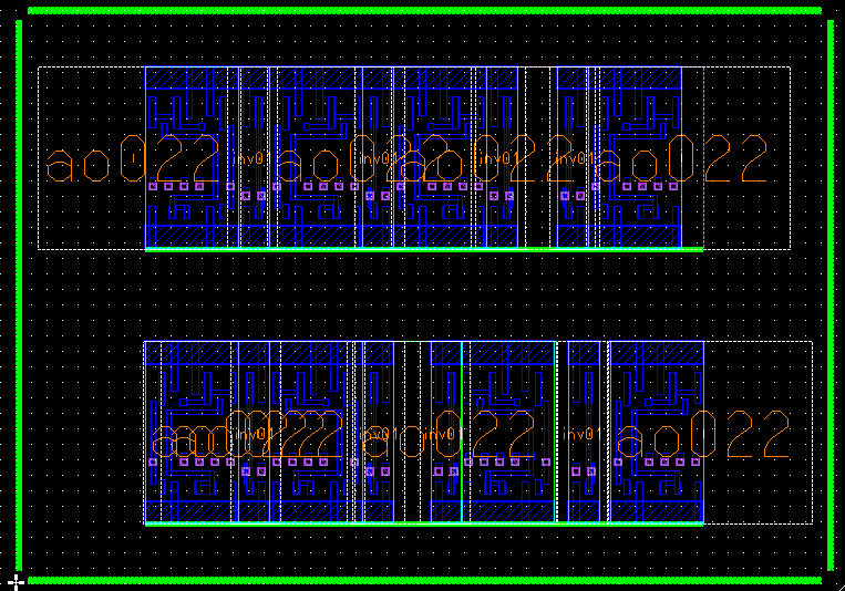
- Select Autoplc->StdCel from the Place & Route palette.
Click OK in the form that will appear, once again allowing all options
to default. You will now see the standard cells placed in the
floorplan boxes. Cell locations are determined by their
interconnectivity. Cells which share connections are placed near one
another. You may wish to experiment with the results obtained thus
far by selecting different Autofloorplan and Autoplace options. It is
hard to see clearly each cell's name because they overlap. One way to
see the name for a particular cell is to select it. Since each
"bounding rectangle" overlaps possibly with more cells you have to
press F3 (cycle selection) a few times until the cell that you are
interested in is only selected. Example.
- Now select Autoplc->Ports from the Place & Route palette.
You can allow the options to default for now, but you may wish to
experiment with them later also. You will see lightly shaded areas
along the port bars at the edge of the layout. By clicking on these
shaded areas you get a message with the name of that particular port.
Alternatively, after you first place the ports automatically, you can
select some of them and place them individually at the location that
you prefer.
- At this point, it is assumed that you have arrived at a
satisfactory initial placement for all the cells of the layout. Prior
to autorouting the interconnect, you may wish to observe a "rats nest"
view of the signals connecting the various cells. This is sometimes
useful to the layout technician for determining sources of routing
congestion. To observe a rats nest of signal connections, select
Connectivity -> Net -> Restructure -> All signal from the top
menu bar. It may look a little messy, but keep in mind that it
doesn't change the layout whatsoever.
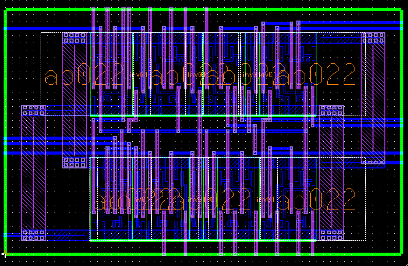
- Now select Autorou->All from the Place & Route palette.
Click OK to accept the defaults. This should route all connections in
the mux design. You will see the cell rows move apart and additional
metal runs appear in the channels between rows. Note that one metal
layer (m1) is used largely for horizontal runs and the other (m2) for
vertical runs. By clicking on individual lines you get a message with
the name of the net that corresponds to each line. Example.
- The autorouter's objective is to complete as many connections in
the design as is possible, without regard for wasted area. For this
reason, a layout compactor is available which "squashes" things
together where there is any little bit of unused space. To take
advantage of this tool, select PR Edit->Compct from the Place &
Route palette. We want to compact in both the horizontal and vertical
dimensions, so do this twice: once down and then again in the
left direction. Do not do this more than once along a given
axis. Not only does it rarely result in improvement, it can lead
to layout errors in some versions of the compactor.
- Save the layout by selecting File -> Cell -> Save Cell ->
Current Context. You may save the layout and exit the IC Graph
session at any time. To re-load the layout later, choose open
from the IC Station palette. If you wish to make changes to the cell,
you must also select File -> Cell -> Reserve Cell -> Current
Context.
At this point, you have completed the automatic layout of your
multiplexer. Many options for viewing the results of this process
exist. Among them:
- Double click middle mouse button to pan view
- "Z" stroke from top to bottom to zoom out, from bottom to top to zoom in
- view->all from the top menu bar to fill the screen with the design
You are encouraged to create the layout of this design using different
options for the floorplanning, placement, routing, and compaction. As
you will see, the resulting layout can be quite different in terms of
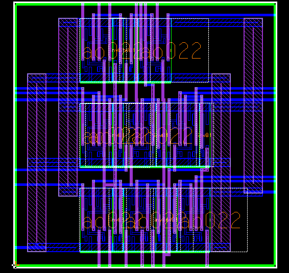
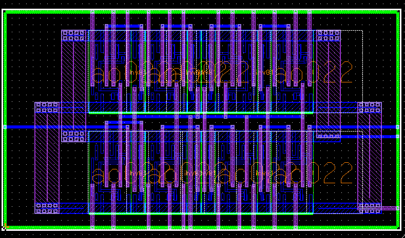
area consumption. For example, the following two layouts were produces
using different IC Blocks options: Example1,
Example2.
Layout Verification
Although the automatic tools performed the layout in the
Correct-by-Construction mode, it is always a good practice to verify
the layout for correctness in terms of both layout design rules and
connectivity, in order to insure consistency between the various tools
used. This establishes a system of "checks and balances" that
increases our overall confidence in the design. We will first check
for layout design rule errors using IC Rules, and then verify
the layout by double checking it against the logic level
representation of the mux logic diagram.
- To return to the main IC Station palette press the right mouse
button in the right side bar and then select root. Now click on the
IC Rules tool and select Check from the IC Rules
palette. A prompt box will appear at the lower left of the screen.
Just click on OK to proceed with the check.
- When the check is complete, design rule errors which exist in the
layout will be reported in the message bar at the bottom of the IC
Station window. You can start with the first one by clicking on
first in the palette, then scroll through the rest by clicking
on next. At this point you may get design rule errors of the
type:
Overlap of N+ and P+ not allowed.
The design rule checker is complaining about p-select and n-select mask
layers being too close. This error is an artifact of how the cell
library was generated. Just ignore it for now. Also, the tool may
report that the p-substrate that we use does not have any substrate
contacts. You can ignore this too at this point.
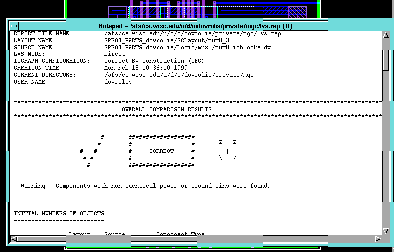
- Next, verify the layout for consistency with the logic-level
schematic of your design. Do this by returning to the main IC Station
palette and selecting the IC Trace(M) (mask-LVS) option. Click
on LVS in the IC Trace(M) palette and in the form which appears
enter the path of the "lvs.vp" viewpoint in the "Source Name" field.
Then click on the Setup LVS button. In the Setup LVS form,
enter:
- Ground Names : VSS GND
Press OK in both forms.
- When the check is complete, the bottom message bar will read
Mask results database loaded and to view the results, you can
select Report -> LVS from the palette. Look for that magic smiley face. If you get that big nasty X
instead, go back and make certain that you have properly set up the
LVS viewpoint and followed the above procedure precisely. When doing
so, look for potential sources of discrepancies between your schematic
and how the layout is generated.
Backannotation and post-layout Quicksim Simulations
You will now backannotate the Quicksim viewpoint with post-layout
capacitive parasitics. The resulting Quicksim simulations will be more
realistic, since they will be modeling interconnect capacitances.
- Return to the main IC Station palette and select the IC
Extract(M) (mask level LVS) option. Click on Lumped for
lumped modeling of the parasitics.
Select "Yes" to specify the schematic source. The "Source name" should
be the viewpoint that you created for IC Trace ("lvs.vp"). Note that
you have to specify the complete path of that viewpoint. Select "Yes"
in the Backannotate button and specify a name for the
backannotation file (select the binary backannotation file).
Click OK and the extraction process will be run. The backannotation
file will be saved in the same directory as the IC Trace viewpoint.
- Now we have to open the Design View Editor to connect the
backannotation to the Quicksim viewpoint. Invoke it by cd'ing to the
directory that contains your "qsim.vp" viewpoint, and type:
dve qsim.vp
- Push the button CONNECT BA and specify the name of the
backannotation file that you created with IC Extract.
- Now, push the Open Sheet button. You will see a lot of
red numbers associated with each pin of the schematic. These numbers
represent the parasitic capacitances (in picofarads) that are
associated with the layout interconnections. You can now save and
close the viewpoint and DVE.
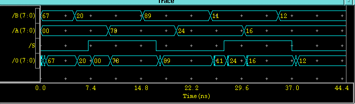
- At this point you can invoke Quicksim and simulate the
backannotated viewpoint (see Tutorial 2). Notice that these
simulations will be more realistic since they take into account both
the cell and the interconnect parasitics. For relatively small
circuits, however, the timing differences between the pre-layout and
post-layout simulations can be too small for Quicksim to produce any
different results. Example.
Before you close IC Station save your completed layout cell
by selecting File -> Cell -> Save Cell -> Current Context.