CREATING AND SIMULATING CMOS DESIGNS
In this tutorial you will learn how to create and simulate 0.8
micron SCMOS circuit designs using the Mentor toolset.
Circuit Schematic
Transistor-based circuit schematics allow more flexibility in the
selection of structures that implement a desired operation. For
example, suppose we want to analyze the following
transmission-gate-based 2-input XOR gate:
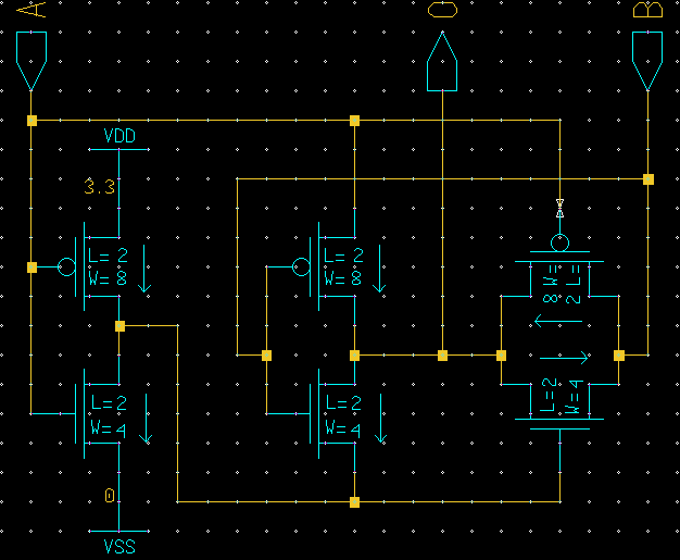
Note that if A=0 the output O is driven by the input B through the
transmission gate. If A=1, the output O is set to the complement of B.
This implements a 2-input XOR gate with only 6 transistors. Also,
note that the VDD supply is set to 3.3V and that all the transistors
have minimum length (2 lambda). Also, all the PMOS transistors have
double width than the NMOS transistors.
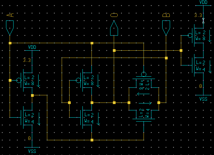
In order to simulate the timing behavior of this structure more
realistically, we will assume that it drives an inverter with the same
transistor dimensions as the XOR gate. The two transistors that make
up this inverter create the load for the output of the XOR
gate. Consequently, the schematic that we want to simulate is as
follows:
Before simulation you need to create this schematic. Run Design
Architect and open a new sheet named, say, tg-xor2. Then
select Choose Symbol and use the Navigator button to go to the
following directory:
$MGC_HEP/lib/sdl
This is the library of MOS transistors for the scmos process.
Design the circuit using the nmos3, pmos3, vdd,
and vss symbols. You can find the port symbols (portin and
portout) in the $MGC_GENLIB library.
Connect these symbols as shown in the above schematic. Do not forget the
following steps:
- Change the VDD voltage from 5V to 3.3V. In order to this, select the
VDD symbol and then modify the value of clicking the right mouse button and
selecting the menu Properties->Modify.
- Change the width of the PMOS transistors in the same way (i.e., select
the transistors and change the width property that determines the
transistor widths; you can do this for either one transistor at a time or
for all of them).
- Name the ports, for example, as A, B, and O.
- Check the design. If you have any errors, fix them. You can
ignore any warnings that relate to the parameter lambda. This
parameter will be specified when we create the design viewpoint.
Save the design and exit Design Architect.
Viewpoint Creation
Before simulation, you need to create a design viewpoint using a
script called sdl_prep. To run sdl_prep, cd
to the directory in which you stored the tg-xor2 design, and
run:
~cs755-1/public/html/mentor/sdl_prep tg-xor2
This will result in a viewpoint directory inside the tg_xor2 directory
called sdl.
Accusim Simulations
You can now run Accusim on the viewpoint you just created. At a
command prompt, cd into the directory that contains your schematic and
viewpoint and type:
accusim sdl
where sdl is the name of the viewpoint created by sdl_prep.
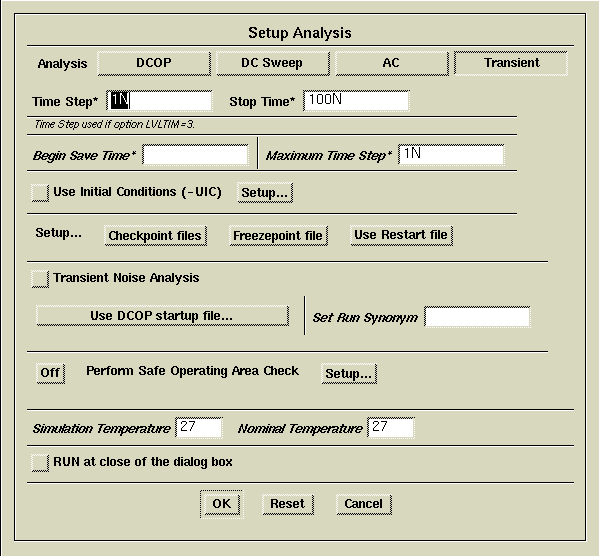
- First setup Accusim for Transient analysis. Click on
the Setup Analysis button, and in the dialog box that results,
select Transient. The Stop Time can be set to 100N (for
nanoseconds), while the Maximum Time Step can be set to 1N. The
form should look like this. Click ok.
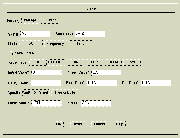
- Now, we have to specify the forces (i.e., input waveforms) for
each input. First, select the input A from the window with the
circuit schematic. Then click on the Add Force icon, and in the
dialog that results select the following:
- Reference (voltage): VSS
- Force Type: PULSE
- Pulsed Value: 3.3
- Delay Time: 0
- Rise Time: 0.1N
- Fall Time: 0.1N
- Pulse Width: 10N
- Period: 20N
The form should look like this. Click ok.
- Now, unselect input A and select input B. Provide the same force
for input B but this time select the delay time to be 2.5N, the pulse
width to be 5N, and the period to be 10N. You may want to experiment
with different force types later. Of special interest is the
PWL (Piece-Wise-Linear) Force Type.
- Now select the two inputs A and B and the output O, and then
click on the Trace button. A form with three traces will
appear.
- Specify the transistor library to be simulated by selecting the
menu File-> Auxiliary Files-> Load Model Library . In the
dialog that results, type in:
$MGC_HEP/technology/accusim/fets.mod.
- Now we are ready to run the simulation. Click on the Run
button, and after a while the traces with the input and output
waveforms will appear:
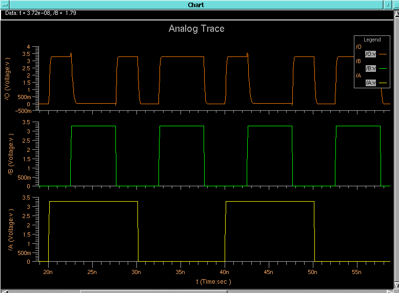
Note that the design is correct, since it behaves as an XOR gate. At
this point you can experiment with different options/utilities of
Accusim. First, you can measure rise/fall times and delays using the
menu WF Measure button in the Result pallete. What are
the rise and fall times for the output O? Also, measure the delay
between each of the inputs A and B and the output O.
- An extremely useful feature of Accusim is `on-the-fly' parameter
changing. For example, you can select one of the PMOS transistors of
the design and then click on the Design Change button. Then,
click on Change Property, and select the width property
of the transistor, giving the new value that you want to simulate.
You can then run the simulation again w/ the new parameters.
Accusim has many more features and capabilities. Of special interest
are the Simulator Setup Options which determine the algorithms
and parameters that Accusim uses in the simulation process. Accusim
can be configured using those options to work with the same accuracy
as SPICE, or just as a switch-level simulator, or in a wide variety of
intermediate accuracy settings.