 |
The
first part of this tutorial will guide you through the process of laying
an inverter using the connectivity editing mode. We will lay the transistors
using the device generator IC station. The second part shows how
to perform Design Rule Check (DRC) and Layout Vs Schematic (LVS) check
in IC station.
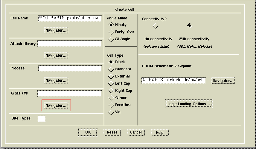
1) Start IC station by typing adk_ic at the
command prompt.
2) Choose create in the menu on the right.
3) In the dialog box that shows up, select connectivity
editing. This mode will maintain the connectivity information from the
schematic. In the box named EDDM
schematic viewpointselect the sdl viewpoint of the schematic. The
sdl viewpoint will be in your schematic directory. Click on logic loading options and select flat
4) Choose Ninety degree angle mode and a name for
your layout. Your dialog box should look like the one in Figure 1.
|
|
Figure 1
6) Select DLA layout->Logic->open. Your schematic
will open in another window. Your screen will look as in Figure 2.
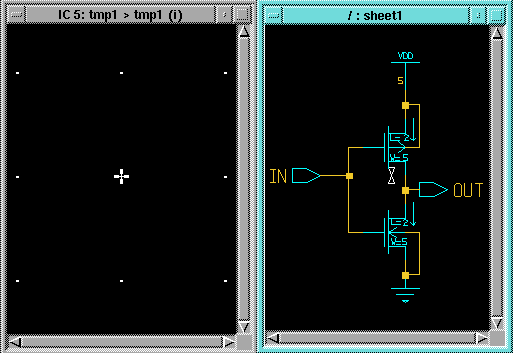
Figure 2 |
7) You can place the transistors all at once or
one by one. To place them all in one go click on the AutoInst
option in the menu on the right. Your layout sheet should appear as in
the figure Figure 3. The yellow lines in the layout window are called overflows.
They
indicate the connections that are to be made. To place the transistors
one-by-one select the fet in the logic window and choose Inst
option in the menu on the right.
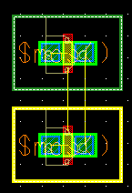
Figure 3 |
8) You might not be able to see some of the features
of the devices or your layout. In order to see the layout in greater detail,
select the desired region and type peek 50. The number 50
is just used for this example. The number actually specifies the number
of levels to be displayed. Refresh your screen everytime you peek view->All
from
the menu on top. The Fets will now look like the ones in Figure 4.
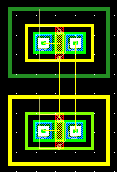
Figure 4 |
9) This problem will occur in few other situations. For example when you add cell. To avoid peeking often you can select Setup->IC->peek on view from the menu on top. This setting will hold through your session. To view the added cell refresh your screen.
10) In Figure 4 you can see an nwell and a pwell. You need to seperate both wells by 18 lambda. You can use a ruler to this. Type add ruler or add ru and drag the ruler. To delete the ruler place del ruler or del ru. There is another way to measure distance. When you zoom in you can see pixels of minimum resolution (mouse pointer cannot be placed between these). The distance between two such pixels is 0.5 lambda. Finally to move Fets or any other objects you can use the Edit->move menu on the top or refer to the tutorial on using strokes.
11) Next step is to place the nwell and pwell contacts.
Just type nwc for nwell contacts and pwc for
pwell contact. Place them as shown in Figure 5.
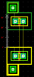
Figure 5 |
Note: When you have large transistors, it is safe to place more contacts.
12) The body of the pmos and nmos have to be connected
to VDD and GND respectively. To do this run a Metal 1 path over the contacts
as shown in Figure 6. This figure shows VDD and GND lines 4 lambda wide.
You might want to use wider power lines.
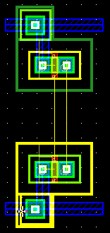
Figure 6 |
Adding paths
To add a path of any layer first select the layer from the top right pallete.
Then select Object->Add->Path from the menu on the top. You
will find a mini dialog box at the bottom of the window. Click on options.
In the dialog box that is displayed enter the width of the path required.
13) Now connect the source of pfet to VDD and that of nfet to GND. Connect the gates of the transistors using poly (you have to add a poly path). Being in the connectivity mode, when you select a net in the layout, the corresponding net in the schematic is highlighted and vice versa. You can use this to identify the source and drain of transistors as well. This also works with overflows.
Note: Use metal connections in one direction. Normally Metal1 is used for horizontal connections and M2 for vertical ones. Following this reduces a lot of trouble in complex layout and also keeps the layout neat. Of course there can be exceptions as in Figure .... Except for such small connections follow this as a rule.
14) Connect the drains of the PFET and NFET using
M2. To make a connection between M1 and M2 a via is used. Type via
to place one as shown in Figure 7.
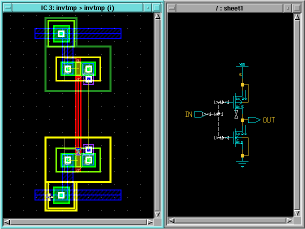
Figure 7 |
15) To make a connection between poly and M1 you need to a poly contact. Type pc to place a poly contact.
16) Final step in the layout is adding ports. Ports
are placed on metal connections. Ports should be of the same metal as that
of the connection on which they are placed. To place ports choose Object->Add->shape
and draw a 4 lambda x 4 lambda square ( Can vary in size) and then choose
Object->make->port.
A small dialog box will appear at the bottom of the window. Enter the values
in this box as per Table 1.
|
|
|
|
|
|
|
|
|
|
|
|
|
|
|
|
|
|
|
|
Table 1
NOTE: You might not be able to see the name of the
ports after performing setp 16. In that turn Setup->IC->Port/Pin
name display to ON. The final layout will look like the one
in Figure 8.
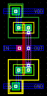
Figure 8 |
1) To run DRC select DRC->check in the DLA layout menu on the right. The you need to select the region to be checked.
2) If there are no design rule violations the status
bar will be similar to the one shown in Figure 9. If there are errors the
Total
results field of the status bar will not be zero.
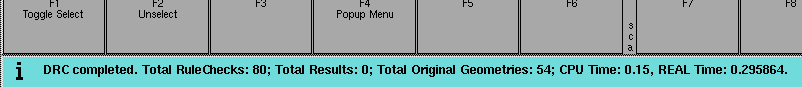
Figure 9 |
3) To see where and what the errors are select DRC->First.
This shows the first error. For other errors keep selecting DRC->Next.
The error will be highlighted in the layout as shown in Figure 10. The
type of error is displayed on the status bar.
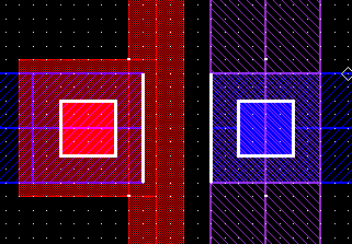
Figure 10 |
4) Once you are done with a check you can delete the results
by selecting DRC->Delete All. This will remove the error
marking from the layout.
The Layout Vs Schematic tool of IC station checks if the layout matches the schematic in various aspects, Nets, Ports and number of nmos and pmos transistors.
1) To run LVS first close the logic window and then select Verifdp->LVS in the IC pallettes menu on the right. In the dialog box that appears choose the sdl viewpoint of the schematic (like the way you had done while creating the layout) in the Source Name text box.
2) Once the LVS check is made the status bar will read "Mark results database loaded". You can view the results of the check by selecting Report->LVS in the ICtrace(M) menu. A smiley face in the reports means your layout has passed the check.
3) Now let us see how to use the LVS report to correct
the errors in our layout. Figure 11 shows a layout with no connection between
the drains of the nmos and pmos. The LVS report will show and incorrect
indication.
Figure 11 |
4) Scroll down to the table named "NUMBER OF
OBJECTS AFTER TRANSFORMATION" as shown in Figure 12. The table shows
the inconsistencies in the number of Nets, Instances and Ports. Here instances
mean transistors. In the component type column mn and mp refers
to nmos and pmos transistors.
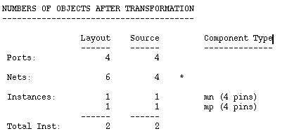
Figure 12 |
5) The table shows that there are two extra net in the layout than in the source. Explanation for this is that in the schematic there is a VDD, GND, a connection between gates, and a connection between the drains of the pmos and nmos, whereas in the layout each drain is now a seperate net and the there is also a dangling port connection.
6) When you scroll down further, you will see a
detailed description of the errors as shown in Figure 13. This table shows
that there is connection between I$1:D and OUT, which is absent in the
layout. Here 'I' means instance, '1' refers to the instance number and
'D' refers to the drain. To identify the FET refered by I$x select a FET
in the logic window and then select Report->Object->Short.
This will give you the I$ reference of the selected device. This can be
done for nets also. The report also shows that there are two drain nets
in the layout which are absent in the schematic. This table also gives
the coordinates of the discrepancies, which can be tracked in the layout
window.
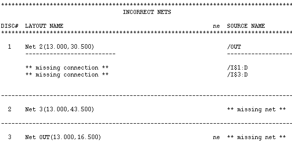
Figure 13 |