Figure 1
This tutorial will take you through the
design process using standard cells. We will first cover the design of
the schematic in Design architect and then make unit delay and nominal
delay simulations in Quicksim. Then we will layout the design in IC station
using the auto-placement and routing tool in IC station. Finally we will
back annotate the layout and perform post layout simulations using Quicksim.
Design Architect
1) Invoke Design Architect using adk_da
2) Open a new schematic as you do for custom designs.
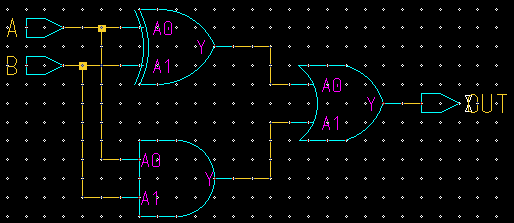
3) Click on Choose Symbol in the setup pallete on the right side. In the dialog box displayed choose $ADK/parts using the navigate button (the one with four arrows).
4) Choose the required components and place them as shown in Figure
1.
|
Figure 1 |
5) Check the schematic using Check->Sheet. You will
get some warnings as shown in Figure 2. Ignore them.
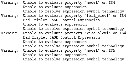
Figure 2 |
6) Run adk_dve <schematic name>
at the terminal.
QuickSim - Unit delay simulation
7) Invoke Quicksim by quicksim <schematic name>/ami05.
8) open your schematic by clicking on open Sheet on the menu on the right side.
9) Now select the inputs and outputs and click on the trace button on the right side menu.
10) convenient way to force inputs in Quicksim is to write a force file. A sample force file (filename.force) for to test this logic circuit is shown below.
delete traces A B OUT
add traces A B OUT
force A 0 0
force A 1 20
force A 0 40
force B 0 0
force B 1 10
force B 0 30
run 50
11) Now simulate the circuit by choosing Setup->Force->From
File and then select your force file. The trace window will look
like the one in Figure 3.
You can add a cursor
by typing add cu.
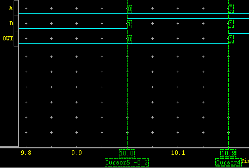
Figure 3 |
Note: You can force a clock input using the following statements.
set clock period 60
force A 0 0 -repeat
force A 1 30 -repeat
The first line sets the clock period and the third line specifies the duty cycle.
12) In order to reset the simulation, choose Run->reset->State. Unselect "Save results waveform DB".
13) Sometimes when you change the force file and then resimulate you
will find that that the circuit is still simulated with the old values.
In that case you need to delete the force by choosing Setup->delete
forces->All signals.
QuickSim - Nominal delay simulation
14) Choose Setup->kernel->analysis and then select delay in the dialog box that appears.
15) Next select Edit->Select->All->Instance. This will highlight the instances in your schematic. For this to work your active window should be the schematic window.
16) Select Setup->kernel->change->typ(in full delay line).
17) Simulate the circuit from the force file as before. The simulation
output is shown in Figure 4. The delay between the inputs and output
is much greater than that of the unit delay case.
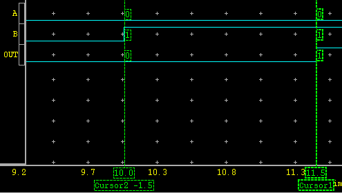
Figure 4 |
Standard cell layout using IC station
18) Invoke IC station using adk_ic.
19) In the create dialog box choose With connectivity and select the layout viewpoint from EDDM schematic viewpoint.
20) Choose Ninety for the angle mode.
21) Select the following :
Attach library: $ADK/technology/ic/ami05
Process
: $ADK/technology/ic/ami05
Rules File : $ADK/technology/ic/ami05.rules
It will take some time to load the libraries.
22) Now select Place & route option from the menu on the right.
23) Now click the autofp option from the menu on the right.
click Ok in the dialog box that appears. your screen will look like the
one in Figure 5.
Figure 5 |
24) Now choose Autoplc->stdcel. This will place the standard
cell as shown in Figure 6.
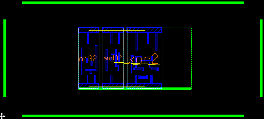
Figure 6 |
25) Now you can use the auto-route tool to make connections. To do this choose Autorou->All.
26) The layout that is generated is not compact enough. To eliminate unecessary space we can use the layout compactor tool. choose Compact. Compact the layout in both the horizontal and vertical directions. So select the down option and then run the compator with the left option. your layout will look the one in Figure 7.
Note: Do not compact more
than once in a given direction.
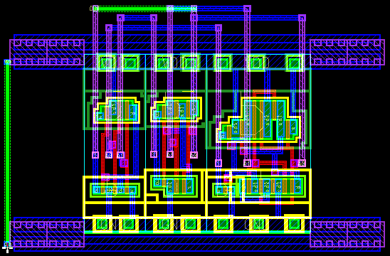
Figure 7 |
27) Run LVS on this layout in the same way as in custom layout.
Post-Layout Simulation using Quicksim
28) To run post layout simulations in Quicksim or accusim we need to back annotate to extract parasitics. This is done in IC station.
29) Select the ICextract(M)->lumped from the ICpalletes menu on the right. Then choose the following in the dialog box that appears:
Write Database : yes
Specify schematic source : yes
Source Name : Full path to your IC trace view point i.e "lvs"
inside your schematic directory.
BackAnnotate : yes
BA name : Give a name to the back annotation file. You
are creating binary backannotation file.
Now click OK. The file will be create in the same directory as the IC trace viewpoint.
30) Now invoke the Design View Editor (dve) by dve ami05. This should be done inside the schematic directory.
31) Now click on Connect BA button in the menu on the right. Select the back annotation file in the dialog box that appears.
32) Save this using File->Save design->With same name->keep existing references.
33) Now invoke quicksim in the same way as pre-layout simulation.
34) When you click on Open Sheet you will see the schematic
window as in figure 8. The numbers marked in red are the interconnect parasitic
capacitances (pico farads) extracted from the layout.
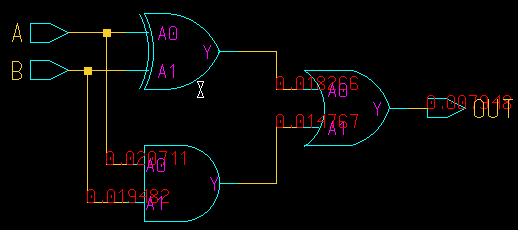
Figure 8 |
35) You can perform the simulations as in the pre-layout case.