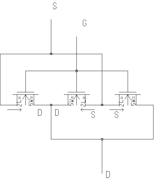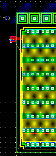
Figure 1
This tutorial will take you through the process of sharing
diffusion regions of transistors and folding large transistors
Diffusion sharing
When the source
or drain 2 transistors of the same type form a net as in Figure 1, their
diffusion regions can be shared. In Figure 1 the 2 nmos devices of the
AND gate have their drain and source connected.

Figure 1 |
On sharing the diffusion regions the layout of both the transistors
will look similar to the one in Figure 2. Since we are in the connectivity
mode we can identify the transistors and their terminals by selecting them
in the layout.

Figure 2 |
How to share diffusion regions?
Create the ICstation sheet in normal fashion. The parameters for sheet creation are repeated below.
Connectivity
: With connectivity
EDDM schematic viewpoint
: SDL viewpoint the of the schematic
Logic loading options
: Flat
Angle mode
: Ninety
Method 1
1) The easiest way to share the diffusion regions is to autoinstantiate the schematic and let IC station figure out the transistors and the regions to be shared.
2) When the schematic of the AND gate in Figure 1 is auto-instantiated
(AutoInst in the DLAlayout menu on the right) we get the layout
similar to the one in Figure 3.

Figure 3 |
3) In Figure 3, we can see that the drains of the pmos are also diffusion shared as they have their drains connected to OUT. We can also note that a active contact is placed in case of pmos alone as their is a connection (OUT) to be made to the shared region.
Method 2
4) The second method is to manually choose the transistors for diffusion sharing and instantiate them. This will instantiate the transistors after sharing the diffusion regions. The regions are correctly picked by ICstation. To do this click on the 2 transistors in the schematic window and select the Inst option from the DLAlayout menu on the right. If you chose the nmos, the layout will be similar to the one in Figure 2.
Method 3
5) The third method is to manually pick the transistors and the regions to be shared. To do this the devices should be placed seperately. Now select the regions to be shared in the layout. In this example we choose the pmos and the their sources.
6) Now select DLAlayout->device->edit->join and
click on OK in the box that appears at the bottom. The layout will similar
to the one shown in Figure 4.

Figure 4 |
7) We can also split shared devices. Just select the shared
region and click on DLAlayout->device->edit->split
and then click on OK in the box that appears.
Folding Transistors
In some circuits due to the required sizing of devices, we end up with
a very odd aspect ratio for the layout. An example of such a circuit is
shown in Figure 5. It is basically an inverter with W/L (nmos) = 1024/8
and W/L(pmos) = 64/8. If this schematic is auto-instantiated, it
will look like the one in Figure 6. The wide p-device can be laid as 'n'
parallel fets so that a better aspect ratio can be achieved. This technique
is called folding.

Figure 5 |
|
Figure 6 |
How does folding work?
Large transistors can be split into smaller ones and then shorting the
corresponding terminals making up the required W/L. In such an arrangement
we can share the diffusion drain and source of adjacent transistors and
then we can short the terminals as shown in Figure 7. This also reduces
the diffusion capacitance. Anyway, we need not be concerned about the whole
process of splitting the transistor and sharing the diffusion regions.
ICstation will do that for us. All we need to do is the shorting of corresponding
terminals.

Figure 7 |
1) Select the gate of the transistor to be folded in the layout and then select DLAlayout->device->edit->fold.
2) A dialog box will appear at the bottom. Number of legs as
required by the box is the number of parallel transistors into which you
would like to split the large device. In this case we enter '8'. The layout
will now look like the one in Figure 8.

Figure 8 |
3) In Figure 8 we can see 8 gates and alternating source and drain (you are in connectivity mode, so you can figure this out). Now we need to short the source, drain and gates of the devices. Let us take the case of shorting the drains. For this you might need to place poly contacts as in Figure 9 for all gates. You can use relative copy (rel copy) for this.
4) Select the block you need to replicate in this case the poly and
the poly contact as in Figure 9. now select DLAlayout->rel copy.
In the box that appears enter the number of copies and the distance between
each. The layout will now look like the one in Figure 10.

Figure 9 |

Figure 10 |
5) In the same way short the drains and sources. The final layout will
look like the one in Figure 11.

Figure 11 |