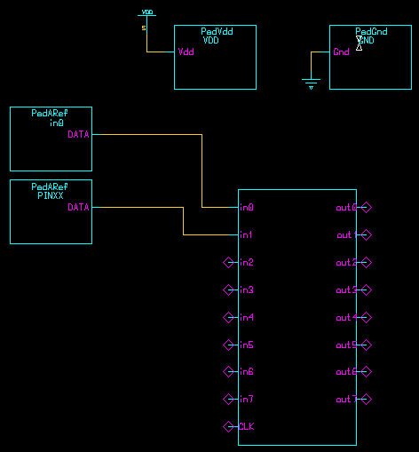
Figure 1
After completing the layout (LVS and DRC) for the entire chip, the final
step is to place the pads for the inputs and outputs. This has to be done
in both the schematic as well as the layout. This tutorial will walk you
through the placement of pads for a sample circuit.
Design Architect:
1) Create a symbol for your final schematic. Open a new sheet in DA and place the symbol.
2) There are three types of pads you will using here. They are signal pads, Vdd pads and ground pads. All signal inputs and outputs are connected to the pad named PadARef. Vdd and ground lines are connected to a pads named PadVdd and PadGnd.
3) All pads are found in $ADK/lib/pads/ami05. For placing a pad
in design architect, use the choose symbol from the right hand pallette.
In the navigation box enter the above path. For example to get a signal
pad enter $ADK/lib/pads/ami05/PadARef. Figure 1 shows a signal
pad connected one of the inputs.

Figure 1 |
4) The Vdd and Gnd pads are placed in similar fashion. These pads need to be connected to Vdd and Gnd respectively as shown in Figure 1.
5) As we can see in Figure 1 the pads have a default name 'PINxx'. Similar to naming ports, each pad should be given a name. To do this just select the name by placing the cursor on it and pressing F1 key. Then right click and choose the change values option to change the name.
6) The final schematic will look similar to the one in Figure 2.
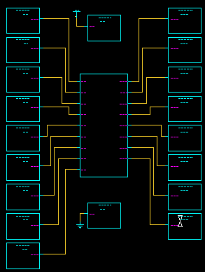
Figure 2 |
IC station:
1) Create a new schematic in usual manner and place the cell (the complete layout).
2) To place a pad, choose the Objects->add->cell option from the menu on the top. In the box that appears are the bottom of the screen entire the following $ADK/technology/ic/pads/ami05/pads/<pad name>. Pad name is PadARef for signal pad, PadVdd for Vdd and PadGnd for Gnd.
3) An important point to note is that all signal pads should get power, hence need to be connected to the Vdd and Gnd pads.
4) Pads are shown in Figure 3. They are signal, vdd and gnd pads in
top-down order. Adjacent pads are abutted. For correct abutting the green
borders of the pads must align as shown in Figure 4.
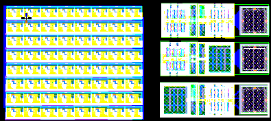
Figure 3 |
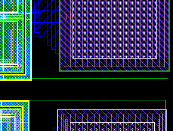
Figure 4a |
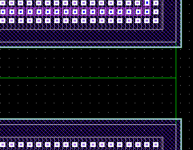
Figure 4 b |
5) Figure 5 shows 20 pads being placed around the cell. The vertically
placed pads on the right side are connected to the Vdd and gnd, as they
are abutted. Others need to be connected.
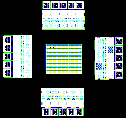
Figure 5 |
6) These connections can be made with the help of a connection pad called
PadFC. This pad can be found in the same location as the other pads. Place
the PadFC pads as shown in Figure 6.
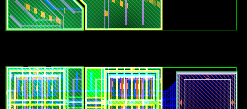
Figure 7a |
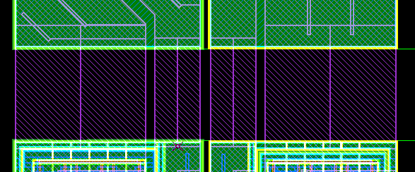
Figure 7b |
7) Connections between the pads will be made with Metal2. The red lines in Figure 7a show the number of metal lines required their placements. Figure 7b shows the completed connection. Do not run the metal lines deep into the pads, it will cause DRC error.
8) After connecting all the pads in corners to PadFC pads, the inputs,
outputs, vdd and ground need to be connected. All signals and power lines
will be connected as shown in Figure 8 which shows the connection for GND.
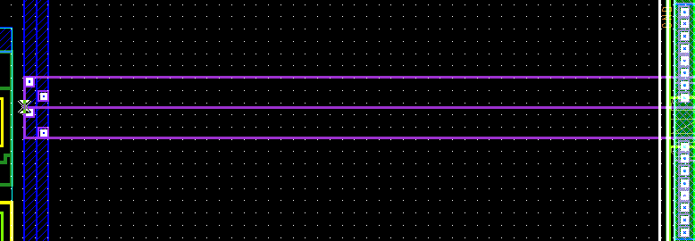
Figure 8 |
9) After completing all the connections. The final layout will look
like the one in Figure 9.
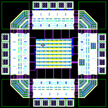
Figure 9 |
10) On running DRC on the final layout you will get few errors. The
number of errors you get should be equal to the number of pads you have.
And the error will like the one shown in Figure 10. Ignore these errors.
|
Figure 10 |