|
Homework 4 [Due at lecture on Mon, Oct 15]
Primary contact for this homework: Pradip Vallathol [pradip16 at cs dot wisc dot edu]
You must do this homework in groups of two. Please write the full name and the student id of each member on every page and staple multiple pages together.
Problem 1 (2 points)
Implement a 2:4 Decoder using only 2-input NAND gates.

Problem 2 (4 points)
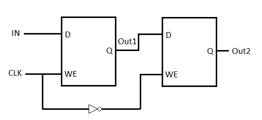
Two Gated D Latches (Section 3.4.2 of your textbook) are connected as shown in the above figure.
The inital state of all the signals at time 't0' is shown in the table below. Fill in the values
of signals 'Out1' and 'Out2', for the given values of 'IN' and 'CLK', at time t1, t2, t3 and t4
where t0 < t1 < t2 < t3 < t4.
| Time |
IN |
CLK |
Out1 |
Out2 |
| t0 |
1 |
1 |
1 |
0 |
| t1 |
0 |
0 |
1 |
1 |
| t2 |
0 |
1 |
0 |
1 |
| t3 |
1 |
0 |
0 |
0 |
| t4 |
0 |
1 |
0 |
0 |
Problem 3 (8 points)
-
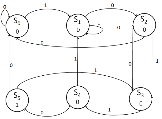
Design a finite state machine (FSM) that recognizes the pattern "10110". The input to the
FSM is a sequence of binary bits in series. When the FSM has "10110" as inputs in
successive bits, it should output 1. Otherwise, the output should be 0. The bits are read
from left to right. For example, for the input sequence 0101101101, the FSM output
should be 0000010010.
S0 is the initial state.
-
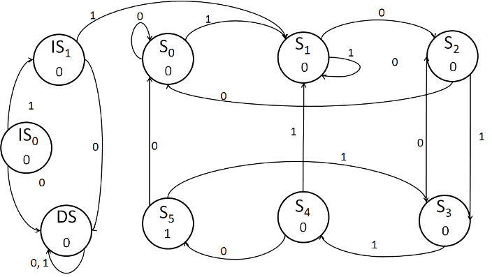
Modify the above FSM such that it accepts only the inputs sequences which start with 11
and still recognizes the pattern "10110" as in part a. For example, for the input sequence
110110110, the FSM output should be 000001001 and for the input sequence 101010110, the
FSM output should be 000000000
IS0 is the initial state, DS is a dead state.
Problem 4 (4 points)
Given that a certain machine has a clock frequency of 80MHz and takes 5 cycles to execute an instruction, find the following:
- Clock cycle period
1/(80 x 10^6) = 1.25 x 10^-8
- Instructions per second
(80 x 10^6) / 5 = 16 x 10^6
Problem 5 (6 points)
Consider an ISA which has the following two instruction formats (instructions in both the formats use the same number of bits):
-
| OPCODE |
DR |
SR1 |
SR2 |
Unused bits (if any) |
-
| OPCODE |
DR |
SR1 |
'N' used bits |
Where DR = Destination register, SR1 = Source Register 1, and SR2 = Source register 2. The ISA has 56 Opcodes and 28 registers.
-
If the value of 'N' is 16 in instruction format (ii), how many bits would be required to represent an instruction?
6 (OPCODE) + 5 (DR) + 5 (SR1) + 16 ('N') = 32
-
For the instruction length calculated in (a), would there be any "Unused bits" in instruction format (i)? If yes, how many "Unused bits" would be present?
32 - [6 (OPCODE) + 5 (DR) + 5 (SR1) + 5 (SR2)] = 32 - 21 = 11
-
If the ISA is redesigned (by still maintaining the property that both the instruction formats have equal lengths), so that instruction format (i) has 0 "Unused bits", what is the maximum unsigned value that can be represented using "'N' used bits" in (ii)?
For 0 unused bits, instruction length = 6 + 5 + 5 + 5 = 21
So N = 21 - (6 + 5 + 5) = 5
Maximum unsigned value = 31
Problem 6 (4 points)
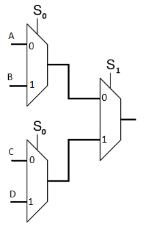
Implement a 4:1 MUX using a minimum number of 2:1 MUXs.
Problem 7 (2 points)
Given an address size of 12 bits with 32 bits stored at each address, what is the total size of accessible
memory (in bytes)?
(2^12 x 32 / 8) bytes = 16384 bytes
|