CS/ECE 552-1: Introduction to Computer Architecture
Spring 2005
Problem Set #2
Due: Wednesday, February 16, 2005
Approximate Weight: 20% of the Homework Grade
You should do this assignment in groups
of two.
Problem 1: 25 points
Design an 8 -by -16-
bit register file using the Mentor
Graphics software. Figure 1 gives the high-level interface. It has
one write port, two read ports, three register select inputs (two for read
and one for write,) a write enable, a read enable, a reset and a clock
input.
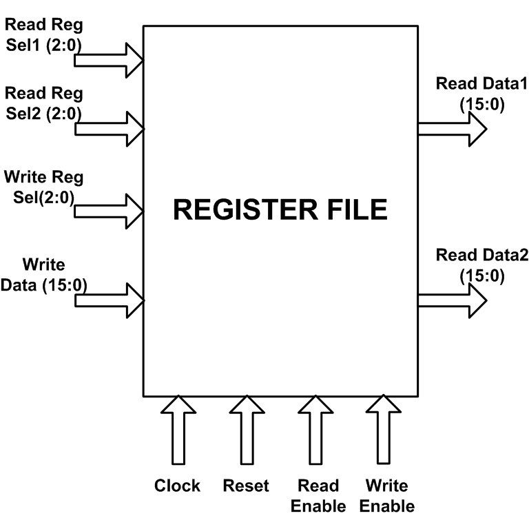
Figure 1: The device for problem 1.
The read and write ports are 16 bits each. The select inputs (read and
write) are 3 bits each. The read or write enable must be asserted (high)
for the corresponding operation to take place. The read enable selects
the read ports, i.e. when the read enable is asserted, the data
from the selected registers will be driven on to the corresponding
read ports. When the read is disabled (i.e. read enable is low)
the read ports must be in tri-state (high impedance state).
The write enable signal selects the write port. The write
must be performed in the first half of the clock cycle (rising edge of
the clock) so that the value may be read in the second half of the clock
cycle.
The reset signal is synchronous and when asserted (active high), resets
all the register values to 0.
You should use a hierarchical design. It is a good idea to design a
16-bit
register first and then put 8 of them together with additional
logic to build the register file. For simulation purposes, any signal that
is wider than one bit should be represented as a bus going into or out
of your system. For a 16-bit bus, there should
not be 16 signals
on your trace output.
Hand in printouts of schematic sheets and symbol sheets for all of your
building blocks along with your annotated simulation traces. The
simulation trace must show that every register can be read and written.
You should also include a case of simultaneous read and write on the same
register and a case of read and write at the same cycle but on different
registers.
Problem 2: 25 points
Design a simple 16-bit ALU using Mentor.
Operations to be performed are ADD, bitwise-AND, bitwise-OR, and bitwise-XOR.
In addition, it must have the ability to invert the B input before performing
the operation. Another input line also determines whether the arithmetic
to be performed is signed or unsigned . Use a carry
look-ahead adder (CLA) in your design. (Hint: First design
a 4-bit CLA. Then use blocks of this
CLA for designing the 16-bit CLA.)
|
OP code
|
Function |
Result |
| 00 |
ADD |
A + B |
| 01 |
OR |
A OR B |
| 10 |
AND |
A AND B |
| 11 |
XOR |
A XOR B |
Table 1: OP code definitions.
The external interface of the ALU should be:
-
Inputs:
-
Data lines A and B (16 bits each.)
-
A carry-in for the LSB of the adder.
-
The OP code (2 bits.) The OP code determines the operation to be performed.
The opcodes are shown in Table 1.
-
An invert-B input (active high) that causes the B input to be inverted
before the operation is performed.
-
Outputs:
-
Data out (16 bits.)
-
OFL (1 bit.) This indicates high if an overflow occured.
-
Zero (1 bit.) This indicates that the result is exactly zero.
In case of logic functions, OFL is not asserted (ie. kept logic low). You
can assume 2's complement numbers.
Use hierarchical design and simulate each block by itself before you
try the complete design.
You should hand in:
-
Schematic sheets and symbol sheets of all the blocks that you designed.
-
Annotated simulation trace output of the complete design.
Pick representative cases for your simulation input.
-
Perform subtraction using your ALU and turn in annotated
trace results showing that it operates correctly. You should subtract
the following:
-
546 - 35
-
-214 - 214
-
-214 - (214 + 1)
-
1 - (-215). Note: This means set A=1 and B="the
2's complement representation for the number -215."
-
Perform arithmetic using your ALU and turn in annotated trace
results showing that it operates correctly. You should perform the following
arithmetic:
-
26 - 25
-
25 - 26
-
16384 - 0
-
1 + (215 - 1)
Problem 3: 20 points
-
Design a 16-bit PC register with the
interface shown as part of Figure 2, but without the PCrd control
line. The function of the control inputs (active high)
is: Reset clears the PC to zero; PCrd should not be
implemented--instead, simply allow the value of the PC register to appear
on PCout at all times; and PCwr loads the address from the
input bus PCin. You may assume that only one control input
is active during any given clock cycle. The Clock input is
marked as being edge-triggered. The write should occur on the leading
edge of the clock, and the output should be available no later than the
trailing edge of the clock.
-
Design a simple incrementer which can
be used to increment the contents of the PC by 1 (note that this is different than the datapath presented in the text, which updates the PC by 4). It should be something
that is cheaper and more efficient than a general adder. You will not
receive full credit for a general adder.
-
Create symbolic versions of the parts you designed above and include them
in the design of the device to calculate the next PC as shown in Figure
2. The control input to the multiplexor is Branch. It
is asserted (high) when a branch target address should be used instead
of the incremented PC. You will want to create another symbol for
the entire device, which you will use in a later assignment.
-
Simulate your design using QuickSim II (base your simulations on the circuit
version of each device, to allow output of internal signals which may help
to show proper operation) and turn in annotated traces, a discussion
of why the trace results show proper operation of each device, and the
circuit and symbolic versions of each device. Your trace results
should include, but not be limited to, the following cases: (Reading the
PC means to show the PC in your trace, and have no changes in the control
lines for one clock cycle, so that the PC value can be easily seen on the
trace.)
-
Reset the PC, read it, and then do an increment followed by a read.
Repeat the increment and read steps 8 times, so that a total of 9 PC values
appear in the trace.
-
Branch to 5FFF16 and then do an increment followed by a read.
This trace only needs to include one PC value. Repeat this test for
the following branch addresses: A12316, BB5616,
and BAAF16.
-
What is a reasonable result when FFFF16 is used in the
above test? Think about the alternatives.
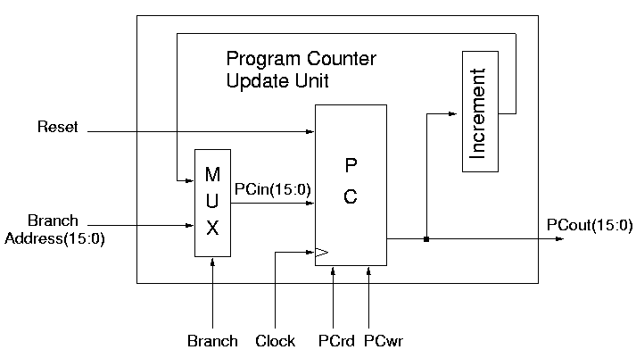
Figure 2: The device for problem 3.
Problem 4: 10 points
-
Do problem 2.13 on page 92 of Patterson and Hennessy (2nd edition.)
Problem 5: 10 points
-
Do problems 2.18 and 2.20 on pages 93-94 of Patterson and Hennessy (2nd edition.)
Problem 6: 5 points
-
Do problem 2.41 on page 101 of Patterson and Hennessy (2nd edition.)
Problem 7: 5 points
-
Do problem 2.44 on page 102 of Patterson and Hennessy (2nd edition.)