Implement a sequence detector in Verilog using a behavioral description. It should be a Moore model machine, in which the output is dependent only on the state in which the circuit is and not the current input. The sequence detector must detect the last three numbers of your student ID, encoded in binary, and zero extended to 10 bits. For example, if the last three numbers are 949, the circuit should detect 11 1011 0101. If the last three numbers are 003, the circuit should detect 00 0000 0011. The circuit output should be high only after the entire sequence has been detected. Compile the Verilog code and build a symbol from it in Design Architect. Simulate the design in Quicksim, showing that it functions correctly.
Please make a note of the sequence that your model detects.
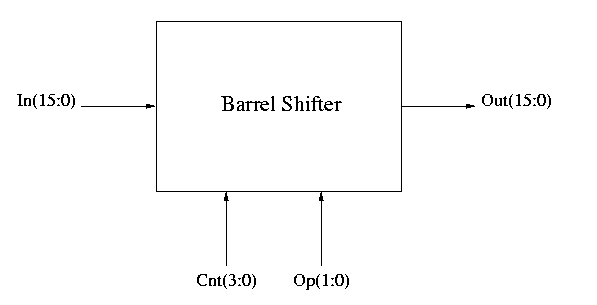
Your design should use only 4-to-1 multiplexors, decoders, and some logic gates for the control.
Simulate your design using QuickSim II. Make a symbolic version of the design which can be used in other circuits. Turn in annotated traces, a discussion of why the trace results show proper operation of the device, and the circuit and symbolic versions of the device. Your trace results should include, but not be limited to, the following cases:
Hand in printouts of all schematics for the circuit, the symbolic version of the circuit, and the annotated traces of the described simulations.
Problem 4.44 on page 330 of H&P
Problem 4.48 on page 330 of H&P
Problem 5
Problem 5.17 on page 429 of H&P
You must download or photocopy the figures in the textbook. Describe any necessary modifications to the datapath or control signals. Show necessary modifications to the finite state machine from Figure 5.42 on page 396 of the text.
Problem 6
This problem is similar to 5.15 from the textbook, except we would like to implement the instruction ADD Rs, [Rt], Rd. This is a "register-memory add" instruction, with bits 31-26 specifying the opcode, 25-21 specifying the register Rs, 20-16 specifying the register Rt, and bits 15-11 specifying the register Rd. The instruction performs an add operation with the contents of register Rs as the first operand, the contents at the memory address contained in register Rt (register-indirect addressing at address M[Rt[) as the second operand, and places the result in register Rd.
You must download or photocopy the figures in the textbook. Describe any necessary modifications to the datapath or control signals. Show necessary modifications to the finite state machine from Figure 5.42 on page 396 of the text. Your solution should not use a lot more clock cycles than what is necessary for the instruction.