CS/ECE 552-1: Introduction to Computer Architecture
Spring 2005
Professor: Guri Sohi
Teaching Assistant: David Mulvihill
Term Project: WISC-FA04 Architecture
Memory System Specification
The WISC-SP05 memory system will provide you with the opportunity to implement three different memory configurations. The first configuration is a single-level of main memory. Your processor will issue read and write requests to a memory controller, which will interact directly with main memory. The second configuration involves interacting with a direct-mapped cache and the third involves interacting with a 2-way set-associative cache.
Note: You have an option of implementing the memory controller by either VHDL, Verilog or a logic circuit.
Part of the WISC-FA04 memory system has been designed for you. You have access to a cache module and a memory module written in VHDL. You will need to create symbols for each of them using Design Architect. Your task is to design a memory controller either by hardware circuit or in VHDL/Verilog and to connect the components together using Design Architect. The controller will take input from the CPU, for instance a read or a write signal. It will then control the other memory modules and output an OK signal to the CPU when the request is finished.
You should try the configurations in order, starting with no cache, moving to a direct mapped cache, and then trying the set associative cache if you have time. No credit will be given if you attempt a harder design without finishing an easier one.
Memory Configuration
1 - No Cache

Figure 1 shows a high level diagram of how this configuration looks. The dashed solid lines are datapaths and the dashed lines are control lines.
What the Memory
Controller needs to do
1.Wait for a request from the processor
2.Set the signals of the memory module for either a read or a write
3.Wait for the memory to complete
4.Signal to the processor that the request is done
Memory Configuration
2 - Direct-mapped Cache
In this configuration, you will build a system that has the following characteristics:
·128KB main memory (1 memory module)
·Direct mapped cache (1 cache module)
·256 entries
·2 word blocks
·1KB capacity
·Write-back scheme

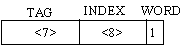
Figure 2 shows the high-level block diagram for this configuration. Due to a lack of money in the WISC-FA04 budget, only one memory module is available for this configuration. Figure 3 shows an address from the CPU and how it's broken down into the cache.
A write-back cache uses the following scheme when processing writes. When the processor writes to a memory location a compare is done to see if the memory location is already in the cache. If it hits, we immediately write the data into the cache and set the dirty bit for the block. If it is a miss, we must first check to see if the block being replaced is dirty. If it is not dirty, we skip directly to loading the cache block we need into the cache. Otherwise, we must first write the replaced block to memory. After the potential write-back is resolved, we read the block we need for our write into the cache from memory. Finally, we write the data into the desired word of the cache block and set the block's dirty bit. Reads are similar. However, the cache sends the data to the core as opposed to receiving it.
What the Memory
Controller needs to do
1. Wait for a request from the processor
2. Perform a compare read/write on the cache
·If it is a hit, signal OK to the CPU. For a read, supply requested data from the cache. For a write, set the dirty bit for the block being written and store the data.
·If it is a miss, go to step 3.
3. If the block being replaced is dirty, write it back into memory, else skip to step 4.
•Get the Tag and Word 0 from the cache
•Combine the Tag, the Index, and the Word bit to form the address to write back to
•Write Word 0 of replaced block to memory
•Wait for memory
•Get Word 1 from the cache
•Write Word 1 to memory
•Wait for memory
•Continue on with step 4.
4. Read the requested block from memory and put it into the cache
•Get Word 0 of requested block from memory
•Wait for memory
•Store Word 0 to cache
•Get Word 1 from memory
•Wait for memory
•Store Word 1 to cache
•If performing a read, supply the requested word to the core
•If performing a write, write the new value into the cache and set it's block's dirty bit.
Memory Configuration
3 - Set-associative Cache
In this configuration, you will build a system that has the following characteristics:
·128KB main memory (1 memory module)
·2-way set associative cache (2 cache modules)
·256 sets
·2 blocks per set
·2 word blocks
·2KB capacity
·Write-back scheme
·Random replacement policy
Figure 4 shows the higher-level block diagram of this configuration. To implement the 2-way set- associative cache, two cache modules are used. One block of the set is stored in one cache, and one block in the other. If more money were available for the project, a second memory unit could be used to interleave memory and allow a full set to be written in parallel.
What the Memory Controller needs to do
The control for this set up is very similar to that of the direct mapped configuration. The only difference is in deciding which block to replace when needed. Here is the algorithm for choosing which cache line to replace:
1. If one block is valid and the other invalid, choose the invalid line
2. If both are valid or both are invalid, randomly choose between the two blocks

A random implementation can be done using a single flip-flop. The flip-flop is set to zero on reset and is toggled on every cache miss. Use the value of the flip-flop to decide which cache block to replace when choosing between the two blocks in a set.
Main Memory Module
The main memory for your processor is a 128KB memory module. There are 216 rows of data, each containing a full word (16 bits) of data. Unlike the RISC processor, WISC memory is word addressable so your program counter should increment by one, not four (or two.)

The block diagram of WISC main memory is shown in Figure 5. The interface for the memory module is described in Table 1.
|
Signal |
In/Out |
Width |
Description |
|
CLK |
In |
1 |
Clock signal. Falling edge triggered |
|
LD |
In |
1 |
Load from file. Active on rising edge. |
|
DUMP_SIG |
In |
1 |
Write contents of memory to a file. Active on rising edge. |
|
WR |
In |
1 |
Write signal. Active high. |
|
RD |
In |
1 |
Read signal. Active high. |
|
AS |
In |
1 |
Address strobe. This signal must be high to read or write memory. |
|
ADDR |
In |
16 |
Address that is being accessed. |
|
DATA_IN |
In |
16 |
On a write, the data that is to be written to the location specified by the address lines. |
|
READY |
Out |
1 |
Goes high when either a write has been performed or the data is available on a read. |
|
DATA_OUT |
Out |
16 |
Data supplied when a read is requested. |
Table 1
To issue a read from the memory module, the AS signal is asserted high in the same cycle the address (ADDR) is driven. The READY signal will go high when the data is available on the DATA_OUT lines. There will be a 4 to 8 cycle delay before a read request completes. Your memory controller should be able to wait an arbitrary number of cycles. As soon as the memory unit asserts the READY signal, the data may be latched. The data will remain valid as long as the AS signal is high and the ADDR and RD lines are stable. Once READY goes high, the memory controller may continue to assert the AS line and immediately drive a different address on the ADDR bus.
To issue a write request, the AS, the WR, the DATA_IN, and the ADDR lines need to be driven on the same cycle. After 4 to 8 cycles, the READY signal will go high indicating that the write has completed. The ADDR and DATA_IN lines should not change until the READY signal goes high. Once READY is high, another read or write request may be started by keeping the AS line high, and changing the appropriate address and control signals. The only exception is that you may not write to the same memory address twice in a row without de-asserting and then reasserting the AS signal.
When the AS signal is low, the DATA_OUT bus will be kept in the high impedance state Z. Signals are sampled on the falling edge of the clock signal so there should be no problems with setup and hold times.
Cache Module
In addition to the main memory module, you have access to a cache module. Figure 6 shows the external structure of the cache module. There are 256 entries in the cache memory. Each cache line has a two-word block. Also associated with each cache line are three bits of state and tag data which are used to decide if a hit has occurred or not.

Figure 6: Shows the external interface to the cache module. Each signal is described in Table 2.
|
Signal |
In/Out |
Width |
Description |
|
CLK |
In |
1 |
Clock signal. Falling edge triggered |
|
DUMP_SIG |
In |
1 |
Write contents of memory to a file. Active on rising edge. |
|
ENABLE |
In |
1 |
Enables the cache. Active high. |
|
RW |
In |
1 |
Read/Write signal. When RW = 0, a read will occur. When RW = 1, a write will occur. |
|
CA |
In |
1 |
Compare/Access signal. When CA = 0, the cache will compare the Index and the Tag to determine if a hit has occurred. When CA = 1, the Tag and Data portions of the cache can be either read or written to depending on the value of RW. |
|
TAG_IN |
In |
7 |
The higher order address bits used to decide if a hit occurred during a compare. |
|
INDEX |
In |
8 |
The middle address bits used to index into the cache memory. |
|
WORD |
In |
1 |
The LSB of the address used to determine whether Word 0 or Word 1 is being accessed in the cache line. |
|
DATA_IN |
In |
16 |
On a write, the data that is to be written to the location specified by the Index and Word lines. |
|
HIT |
Out |
1 |
Goes high during a compare if the tag at the location specified by the Index lines matches the TAG_IN lines. |
|
VALID |
Out |
1 |
During a compare, this signal goes high to indicate that the cache line contains valid data. The valid bit is set to 1 by the cache when an Access/Write occurs to that cache line. |
|
DIRTY |
Out |
1 |
During a compare, indicates whether the cache line has been written to. On a Compare/Write, the cache sets the dirty bit to 1. On an Access/Write, the dirty bit is reset to 0. |
|
TAG_OUT |
Out |
7 |
On an Access/Read, the value of stored in the tag for the given cache line is driven on to this bus. This value is needed during a write back. |
|
DATA_OUT |
Out |
16 |
Data supplied on a read hit or a compare. |
Although there are a lot of signals for the cache, its operation is pretty simple. When ENABLE is high, the two main control lines are Compare/Enable (CA) and Read/Write (RW). Here are the four cases:
Compare Read (CA = 0, RW = 0)
This is case is used when the processor requests data from the memory system. The TAG_IN, INDEX, and WORD signals need to be asserted when the ENABLE signal is asserted. On the falling edge of the clock, either a hit or a miss will occur. If a hit occurs, the HIT line with be raised to one and the DATA_OUT will contain the valid data. If a miss occurs, the HIT line will not be raised to one but the VALID and DIRTY outputs will be available so that you can decide what to do next. Since a compare occurs in one clock cycle, by the rising edge of the next clock cycle you will know whether a hit or a miss has occurred.
Compare Write (CA = 0, RW = 1)
This case occurs when the CPU wants to store data to an address. The DATA_IN, TAG_IN, INDEX, and WORD lines need to be asserted when the CA, RW, and ENABLE lines change. On the falling edge of the clock cycle, either a hit or a miss will occur. If a hit occurs, the HIT line will be raised to one and the data will have been written. The dirty bit for that cache line would also have been set. If a miss occurs, the HIT line will not be raised to one but the VALID and DIRTY outputs will be available so that you can decide what to do next. Since a compare occurs in once clock cycle, by the rising edge of the next clock cycle you will know whether a hit or a miss has occurred.
Access Read (CA = 1, RW = 0)
This case occurs when you want to read the tag and the data out of the cache memory. You will need to do this when a cache line needs to be written back to memory. The INDEX and WORD signals need to be asserted when the CA signal goes from zero to one. On the falling edge, the vale stored in the tag and the data in either Word 0 or Word 1 will be available on TAG_OUT and DATA_OUT.
Access Write (CA = 1, RW = 1)
This case occurs when you bring in data from memory and need to store it in the cache. The INDEX, WORD, TAG_IN, and DATA_IN signals need to be asserted when the RW signal goes from zero to one. On the falling edge of the clock, the values will be written into the specified cache line. Also, the valid bit will be set to one and the dirty bit set to zero.
Implementation Notes
The memory module file can be found in: ~cs552-1/public/html/Project/VHDL/mem.vhdl
The cache module file can be found in: ~cs552-1/public/html/Project/VHDL/cache.vhdl
You need to edit each file to point to your input and output files