UW-Madison
Computer Sciences Dept.

CS/ECE 552 Introduction to Computer Architecture


Spring 2012 Section 1
Instructor David A. Wood and T. A. Ramkumar Ravikumar
URL: http://www.cs.wisc.edu/~david/courses/cs552/S12/

CS/ECE 552 : Introduction to Computer Architecture
Spring 2012
Prof. Wood
Problem Set #5

Due: April 11th, 2012

Assignment is split between project group and individual work

You can find the PDF copy of Discussion Session 8 here

You can find the PDF copy of Discussion Session 9 here

An example FSM for the direct mapped cache here

  • Example waveform on running mem1.addr in a direct mapped cache is (A load miss to address 472 [(in HEX 01D8). In the trace we have provided, the address is 348] here
  • Example waveform on running mem2.addr in a direct mapped cache is (A load miss to address 472 and then a load Hit to same address [(in HEX 01D8). In the trace we have provided, the address is 348] here
  • Example waveform on running mem3.addr in a direct mapped cache is (A load miss to address 348 and then a store Hit to same address [(in HEX 015C)] here

    • Homework is due at start of class
    • Problems 1 - 2 MUST be done with your project group    (handin verilog to “HW5”, report  portions on paper)
    • Problems 3 - 5 MUST be done ALONE                                  (all paper)
    • No exceptions to the above handin rules will be allowed.
    • You must abide by the Verilog file naming conventions
    • All verilog code must pass Vcheck
    • Each problem must be in its own directory
    • If a problem requires files from a different directory, then create a copy of the file in each directory.

    1.  Problem 1 -35 Points

    FIRST COMPLETE DIRECT-MAPPED CACHE BEFORE MOVING TO SET-ASSOCIATIVE CACHE

    (Download this tarball for easy access to all required files for problems 1&2.)

    You will implement a hierarchical memory system in Verilog that consists of a level-1 write-back cache with write-allocate policy and stalling memory. The system should use a direct-mapped cache and a four-banked, four-cycle memory. See the project modules provided page for the Cache module and four-banked memory module. Blocks are 4 words wide and the system is byte-addressable, word-aligned.

    The top level module that you will develop is as follows. verilog template source for mem_system.v

    module mem_system(/*AUTOARG*/
       // Outputs
       DataOut, Done, Stall, CacheHit, err,
       // Inputs
       Addr, DataIn, Rd, Wr, createdump, clk, rst
       );
    
       input [15:0] Addr;
       input [15:0] DataIn;
       input        Rd;
       input        Wr;
       input        createdump;
       input        clk;
       input        rst;
    
       output [15:0] DataOut;
       output Done;
       output Stall;
       output CacheHit;
       output err;
    
       /* data_mem = 1, inst_mem = 0 *
        * needed for cache parameter */
       parameter mem_type = 0;
    
       // <<<your code here>>>
    
    endmodule // mem_system

    A top-level module called mem_system_hier.v is also provided which instantiates the clock generator and mem_system inside it. verilog source for mem_system_hier.v

    The tarball listed above contains two testbenches, with a reference memory module, and loadfiles to initialize your memory.


    Important Notes:

    • This module will also handle internal errors.

    • The system should ignore new inputs when it is stalled (not an error). Timing will be an important part of this problem; Designs that stall longer than necessary will be docked points.

    • The Done signal should be asserted for exactly one cycle. If the request can be satisfied in the same cycle that data should be presented, Done should be asserted in that same cycle.

    • The CacheHit signal denotes whether the request was a hit in the cache.

    • The memtype parameter decides whether this is an instruction or data cache which is used to generate the names for the dump files.

    To complete this problem, you will need to determine how the internal components are arranged and will have to create a cache controller FSM. See the description of the cache module for hints on how this should be done. You can chose to implement either a Mealy or Moore machine, although I recommend using a Moore machine as it will likely be easier to create. Be forewarned that the resulting state machine will be relatively large so get started early.

    The testing for this module should be extensive. You will need to verify that the design works correctly during hits, misses, writebacks, and refills. Also be sure to check the design under various main memory stall conditions.

    For extra credit, you can improve your performance by adding a two-entry store buffer so that it is possible for writes to complete in one cycle. The extra credit will not count if the standard system is not working, so be sure to thoroughly test your design before thinking about moving on.


    Instantiating the cache modules:

    This is the methodology I suggest for instantiating your cache modules, so the naming conventions are the same for everyone.


    Somewhere in mem_system.v:

    cache # (0 + memtype) c0(....)


    This will guarantee that when this module is finally connected to your processor, your instruction and data memory will create separate dump files. See the Cache module section for details.


    Verification

    Verification is an important part and significant challenge for this problem. You are provided with two testbenches:

    • mem_system_perfbench.v: This is a more carefully constructed testbench that is meant to check the performance of your design. For example, is your cache reporting cache hits and misses correctly. Are the requests being serviced in the correct amount of time etc. This testbench takes as input a memory address trace in a file called mem.addr. This file must be in the same location as your verilog files. An example mem.addr file is provided. The format of the file is the following:

      • Each line represents a new request

      • Each line has 4 numbers separated by a space

      • The numbers are: Wr Rd Addr Value

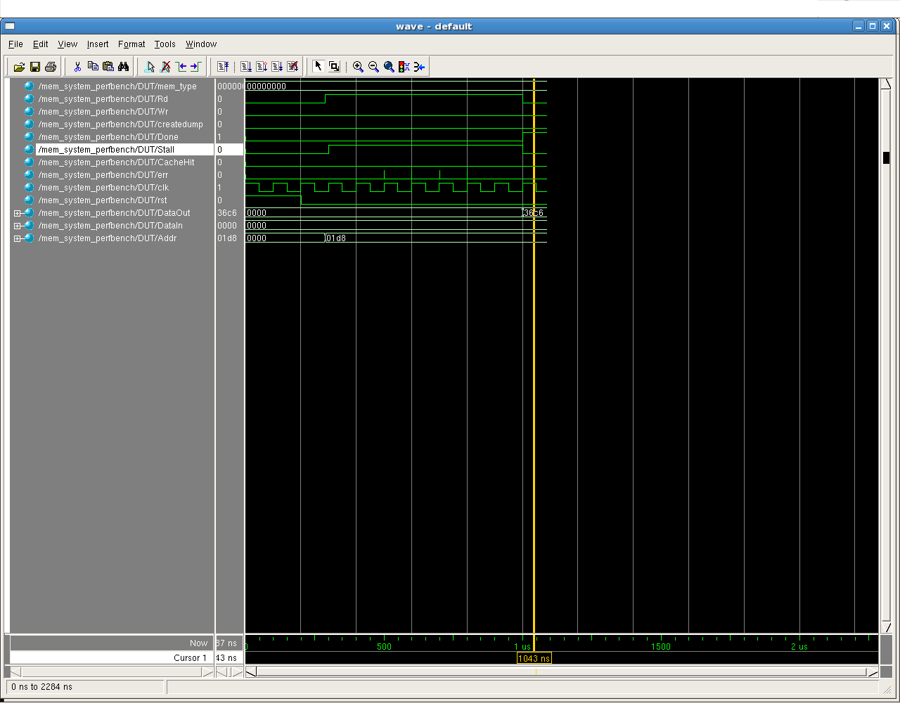
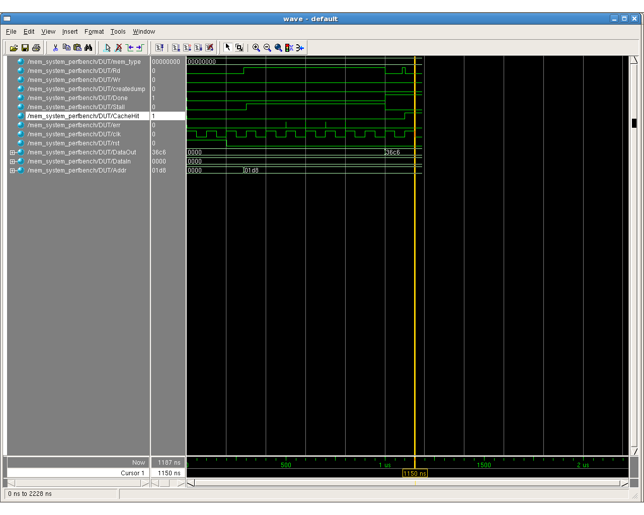
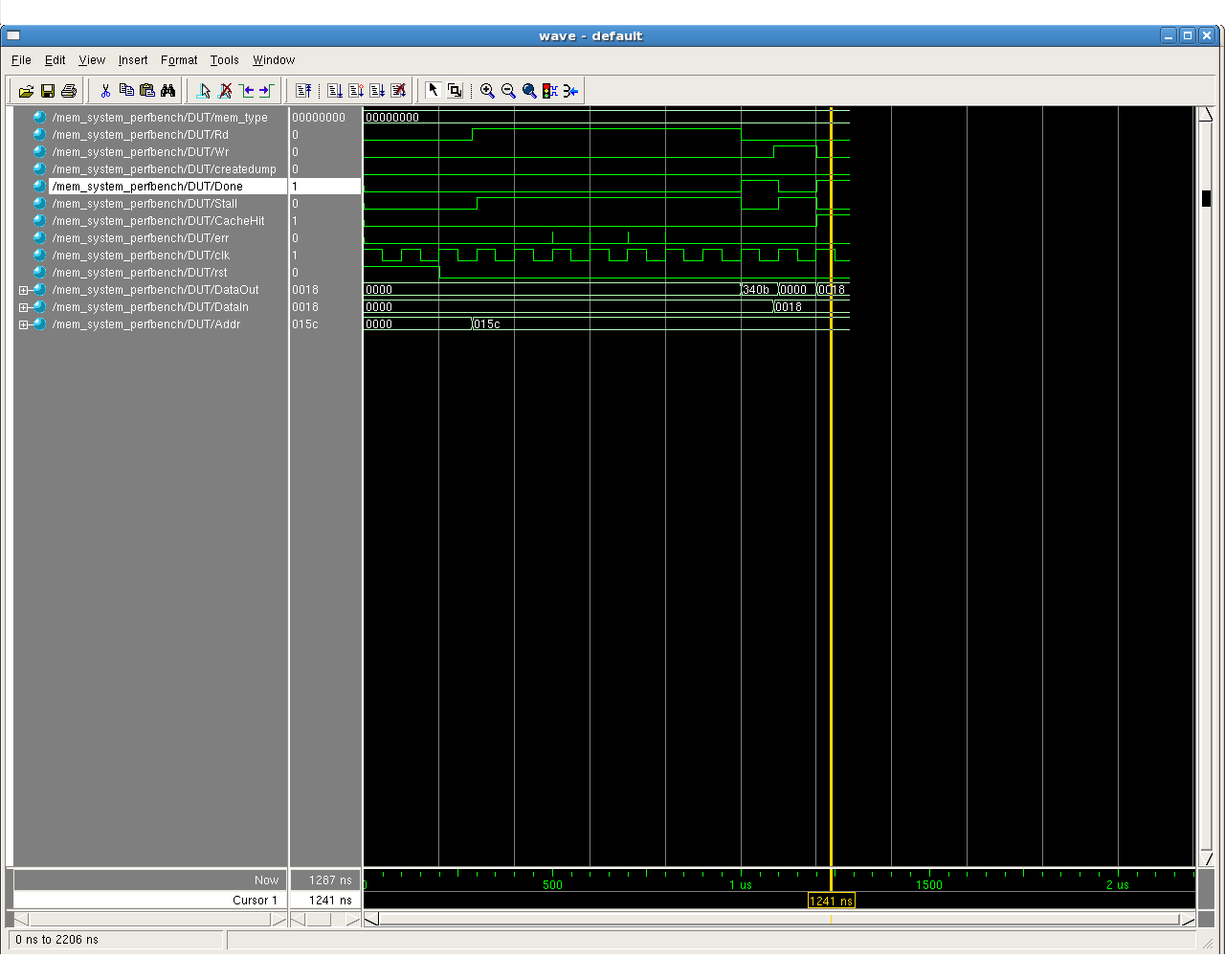
    You must write different address traces to test your module and prove that it does implement the cache correct. Determining what to test and show is an important part of this problem. Carefully document and show in your homework, what cases you are testing. Pick representative inputs from this testbench, by examining the waveforms. You must handin annotated waveforms to prove that your design works correctly during hits, misses, writebacks, and refills.

    To run this testbench:

    wsrun.pl -addr mem.addr mem_system_perfbench *.v
    • At least 5 traces are required.

    • Do not start randomized testing until you have proven to yourself that your cache shows some basic functionality.

    • mem_sytem_randbench.v: This is a completely randomized testbench that stresses the functional correctness of your design. You must run this testbench, which will print a log of addresses and statistics on the number of hits to the cache. Contact the TA for questions about the testbench. Your module must pass this testbench. The output log is saved in a file called transcript. Copy this file as randbench.log and include in your handin. Specifically this testbench does the following:

    1. full random: 1000 memory requests completely random

    2. small random: 1000 memory requests restricted to addresses 0 to 2046

    3. sequential addresss: 1000 memory requests restricted to address 0x08, 0x10, 0x18, 0x20, 0x28, 0x30, 0x38, 0x40

    4. two sets address: 1000 memory requests to test a two-way set associative cache. You should get predominantly hits to to the cache.

    After every set of 1000 requests, you will see a message like the following:

      LOG: Done two_sets_addr Requests: 4001, Cycles: 79688 Hits: 562

    To run this testbench:

    wsrun.pl mem_system_randbench *.v

    Pay careful attention to the sequential address and the two sets address traces. You can look at the testbench to see what sequence of address this is. You should be able to estimate how many hits your cache should report on them.


    Synthesis

    As with other homeworks you must synthesize your design. You must turn in the entire synth directory and make sure your total combinational area is non-zero.


    (If you implemented the extra credit, please make a note.)

    Submit on Paper:

    1. Turn in neatly and legibly drawn schematics of your design. Your design hierarchy should be clear in this schematic.

    2. A state diagram of your cache controller.

    3. State Transition Table

    4. Fill in the table for the 8 regression address traces: HW5 Problem1 address trace table

    5. On the handwritten homework you turn in, fill in the following synthesis info:

      1. Total area:

      2. Worst case slack:

    Submit Electronically: (directory prob1)

    1. All your verilog source code.

    2. For the mem_system_randbench testbench, the log output in a file called randbench.log.

    3. For the mem_system_perfbench testbench, all additional trace files your wrote. Each such file should end with the extension .addr

    4. The entire synth directory

    5. Make sure to use mem_system.syn.v, and the 3 report files (area_report,timing_report,cell_report) are present

    6. Make sure that in the area report no cell has an area of zero


    2.  Problem 2 -20 Points

    Implement your 2-way set associative cache which is required for the project. See the Cache module page. Replace your direct-mapped cache in the above problem with this 2-way set associate cache. (We will be following a pseudo-replacement policy for the set-associative cache. Please refer to the Cache module link above)

    Instantiating the cache modules

    This is the methodology I suggest for instantiating your cache modules, so the naming conventions are the same for everyone.


    Somewhere in mem_system.v:

    cache # (0 + memtype) c0(....) cache # (2 + memtype) c1(....)


    This will guarantee that when this module is finally connected to your processor, your instruction and data memory will create separate dump files. See the Cache module section for details.

            Parameter Value     File Names
            ---------------     ----------
                   0            Icache_0_data_0, Icache_0_data_1, Icache_0_tags, ...
                   1            Dcache_0_data_0, Dcache_0_data_1, Dcache_0_tags, ...
                   2            Icache_1_data_0, Icache_1_data_1, Icache_1_tags, ...
                   3            Dcache_1_data_0, Dcache_1_data_1, Dcache_1_tags, ...

    Pay careful attention to the sequential address and the two sets address traces from mem_system_randbench. You can look at the testbench to see what sequence of address this is. You should be able to estimate how many hits your cache should report on them.


    Submit:

    1. Follow directions for Problem 1

    2. Put files in a folder called prob2

      (on paper)

    3. Fill in value for the 6 address traces for the 2-way set associative cache: HW5 Problem2 address trace table

    4. For mem_2way7.addr print the text output of simulation with all the LOG messages. You should use this simulator described here. These message should denote the hit/miss for each request. You should explain in handwritten notes the reason for each each hit/miss


    #END GROUP WORK#


    3.  Problem 3 – 15 Points

    Consider a direct-mapped cache with 32-byte blocks and a total capacity of 512 bytes in a system with a 32-bit address space. Assume this is a byte addressable cache.

    1. Indicate which bits of an address in this machine correspond to the tag, index, and offset, respectively.

    2. For the sequence of addresses below, indicate which references will result in cache hits and which will result in cache misses. If it does result in a miss, mark whether the miss was a compulsory, capacity, or conflict miss. Assume the cache is initially empty. (All valid bits are set to 0)

    3. Show the final contents of the address tags at the end of execution.

    4. Explain what can be done to improve each type of miss.

    0x0001b596  
    0x000092e8 
    0x00000ef4
    0x00004182  
    0x0000780a  
    0x0000a690  
    0x0000408e  
    0x0000a798  
    0x00007800  
    0x000092fc  

    4.  Problem 4 – 15 Points

    Re-do problem 3, but using a two-way set-associative cache. When replacing a block, the least-recently-used block is chosen to be replaced. Everything else (block size and total capacity) remains the same.

    Determine the speedup over the direct-mapped cache in problem 3. Assume both caches can be accessed in 1 cycle, that the CPI without misses is 1.0, and that the miss penalty is 25 cycles.


    5.  Problem 5 - 15 Points

    Consider a cache with the following characteristics (valid-1 bit; dirty-1 bit and LRU-2 bits):

    • 64-byte blocks

    • 5-way set associative

    • 512 sets

    • 41-bit addresses

    • writeback

    • LRU replacement policy

    1. How many bytes of data storage are there?

    2. What is the total number of bits needed to implement the cache?


    Handin Instructions

    Hand in your homework using the CS handin program.

    • Make a folder for each problem (prob1, prob2)
    • Each folder should contain all the verilog files for that problem.
    • name and signals for the top level module should be as indicated for each problem
    • tar these 2 folders to 'cs username'.tar [example : tar cvf ram.tar prob1 prob2]
    • Copy the tar file over to an empty folder and submit it using handin documentation [example: mkdir ram; mv ram.tar ram]
      * <class_name> cs552-1
      * <assignment_name> HW5
      * <directory_path> 'location_of_the folder_you_created'

     
    Computer Sciences | UW Home